System Maintenance occurs every Friday.
System Maintenance occurs every Friday.
The term "decapsulation" can refer to a procedure performed on either hermetic devices or polymer encapsulated devices. Decapsulation is the removal of a cap, lid, or encapsulating material from a packaged integrated circuit by mechanical, thermal, or chemical means. Decapsulation exposes the integrated circuit for the purpose of further analysis. Techniques should be compatible with the particular packaging configuration in order to minimize complications from introduction of foreign matter or damage to the device.
The user can choose a solution from several suggested techniques. Some decapsulation techniques seem as basic as breaking a package open or heating to melt a soldered seal. Chemical removal of polymeric encapsulating material with acid is standard. Specific techniques are included for ceramic or metal hermetic packages, Transistor Outline (TO) "cans," CERamic Dual In-line Packages (CERDIP), and polymer encapsulated (plastic) packages.
Decapsulation is performed to gain access to the package cavity and/or surface of a device for the purpose of further analysis. In the case of a hermetic device, removal of the lid permits visual inspection for foreign material, corrosion, mechanical damage, or other workmanship and processing issues. Removal of polymeric encapsulating material from a plastic packaged part also reveals the IC surface. It allows FA techniques--such as high resolution optical microscopy, electrical probing, and electron beam-- to become possible and opens the door for removal and deprocessing of the IC.
Decapsulation techniques depend on packaging configuration. The user may choose an appropriate solution from the following suggestions.
Flat metal lids are common on ceramic and metal packages used for hermetic, high reliability, and military applications. Typically, the metal is Kovar plated with nickel and gold. For integrated circuit applications, the lids are usually soldered to a plated, thick-film seal ring layer (on ceramic packages) or to a plated metal seal frame (on metal and certain ceramic packages). The most common solder is a eutectic gold-tin alloy which has a liquid temperature at 280oC.
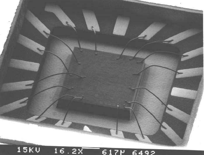
An obvious opening technique is to remove such a lid is chiseling with a razor knife aided by a small hammer. The package should be supported in a small vice. A small cut is made in the solder fillet at a perimeter corner in order to guide the blade between the lid and the seal ring. The chisel-edged blade can then be carefully tapped into the seal, avoiding contact with wirebond loops or the die surface. The brittle nature of the solder at room temperature will usually cause the lid to break free from a thick film seal ring layer on a ceramic package. Sometimes, the thick film layer will be lifted from the ceramic. On a metal seal frame, there may be a tendency to gouge the seal frame, and extra care is needed to keep the blade from cutting into the solder seal.
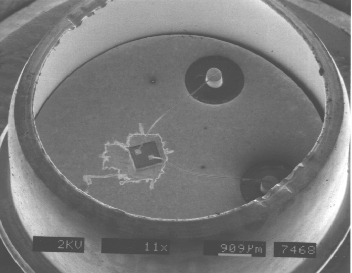
One disadvantage of this technique is the seeding of foreign material associated with the fracture into the package cavity. This foreign material is discernible from solder balls, but not from certain other suspicious particles. Common safety awareness necessitates the use of safety glasses or a face shield to protect eyes and face and care that sharp edges do not cut skin. Figure 1 shows a view of the cavity of a device successfully delidded without damage to wirebond loops. Removal of a soldered metal lid by heating is also an option. Temperatures of about 335oC will be required. The temperature required to remove a lid increases as gold plating is taken into solder solution. It is important that the effect of these temperatures on the rest of the device be understood. Foreign material generated in this step is limited to solder balls.

Other techniques which could be used include the milling, grinding, or sawing of the seal in a machine shop environment. The part should be protected from electrostatic discharge and gross mechanical damage, but the creation of particulates is unavoidable.
A CERamic Dual In-line Package (CERDIP) consists of a sealing glass layer sandwiched between a ceramic base and cover. The electrical leads are embedded in a heated soft glass layer on the base prior to die attach and wirebonding. The cover is subsequently mated to this assembly by heating to about 400oC. Figure 2 shows a cross sectional view of this structure.
A technique for decapsulating such a package is to score the glass layer with a diamond scribe point at the perimeter of the package. This procedure, which can be done manually or automatically, directs stress concentration and and applies a chisel action to separate the cover from the base. Automatic equiptment used to perform this step consists of a clamping platen that forces a sharp edge into the seal area as a leadscrew is turned.
A disadvantage of this technique is that it is a bit like cracking a nut open and the results are somewhat unpredictable. It is possible to fracture one or both of the ceramic halves, and the leads may be broken. Nevertheless, it is the most common method. The chances of success can be enhanced by securing the leads to the body with epoxy prior to breaking. Figure 3 shows a CERDIP package which was decapsulated by breaking the cover off the package. A second method is to thin the ceramic cover by grinding until only a fine web remains over the IC. This web can then be broken at the perimeter and lifted from the package using a tweezer.
These packages consist of a header that acts as a base welded to a thin cap. Electrical feedthroughs in the header provide interconnect to the device inside. Opening this package can be accomplished with a commercial device resembling a can opener. A sharp, rotating circular blade perforates the metal cover at its perimeter and the top drops off. Figure 4 shows a package which was opened with a "can opener" device. A small Jeweler's saw could also be used to cut the cover so the top can be removed. Any cutting should be done with an awareness of the contents of the package to avoid accidental contact of a blade with the die or its interconnect.
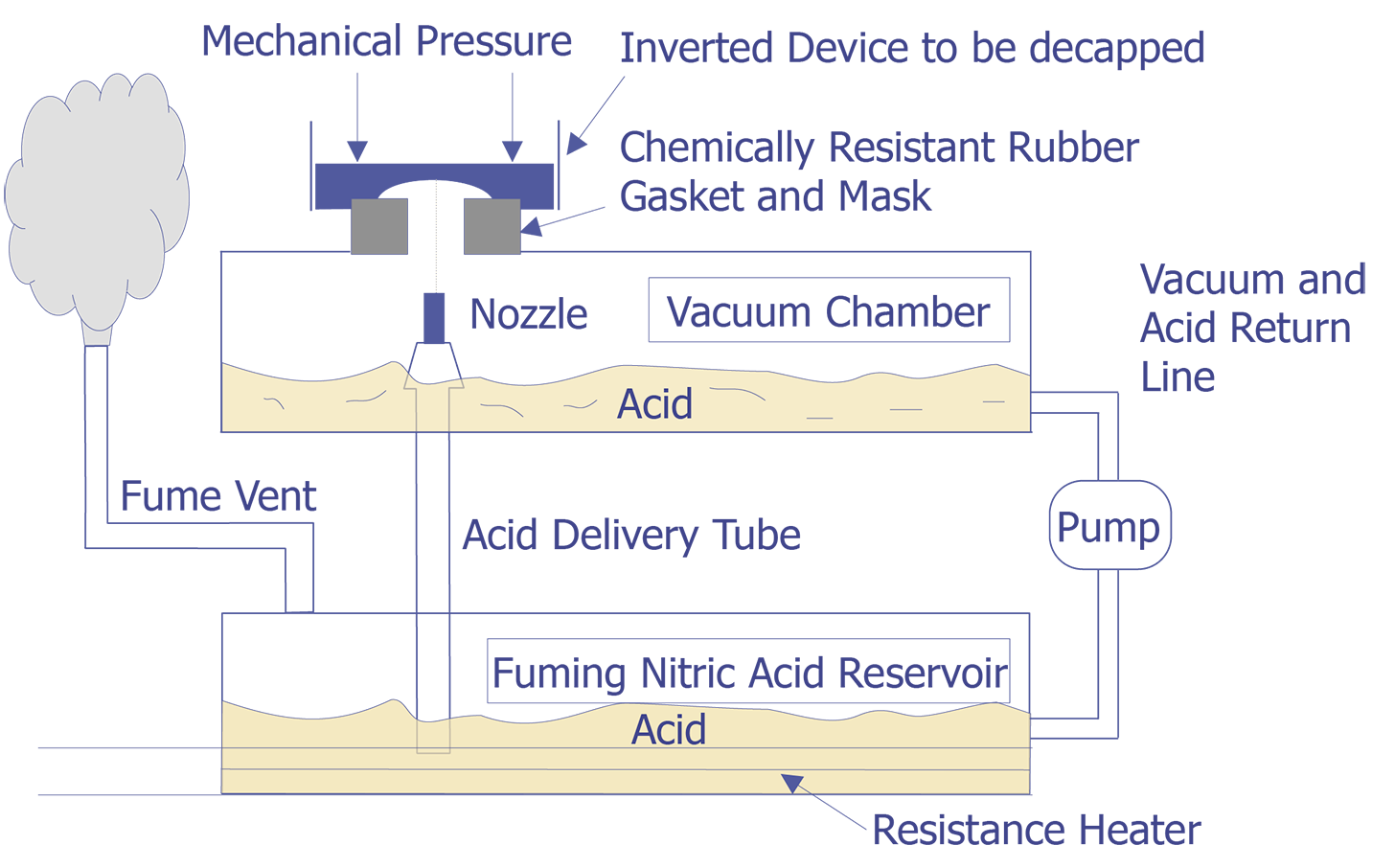
The preferred technique for decapsulating plastic encapsulated parts is to use a jet etch apparatus, which is commercially available from a few sources. This type of equipment directs a jet of heated acid toward the surface of the package in an etch head, causing a chemical reaction and erosion of the encapsulation, eventually exposing the die. The choice of acid depends on the type of polymer which is being removed. Fuming nitric acid is reported as a specific solvent for phenolic epoxies, whereas fuming sulfuric is specific to anhydride epoxies (Ref. 1). Models are available for fuming nitric acid, concentrated sulfuric acid and mixtures of fuming nitric and fuming sulfuric acid. When concentrated sulfuric acid is used, it is heated to 280-290oC. Fuming nitric acid and mixtures are used at a temperature of 75-80oC.
Because the acid stream is concentrated over the die, the leads and the rest of the package body remain intact. The mechanical removal of polymer material in advance of etching is usually unnecessary, and the entire die can be exposed, leaving the wirebonds intact. The automatic nature of the equipment makes it possible to have process recipes for time and operating conditions in order to remove guesswork and operator effects. The small reaction volume means that small amounts of acid are usually heated and in use.
Both positively pumped systems and vacuum aspiration systems are available. An advantage of the vacuum aspiration system is the automatic stoppage of the jet if the seal between the apparatus and the package is broken. An advantage of the pumped system is the ability to continue the process if a sidewall of a small package is breached. All such apparatus must still be used in a fume hood and appropriate protective personal equipment (gloves, safety glasses, face shield, and apron) must be used when handling acids.
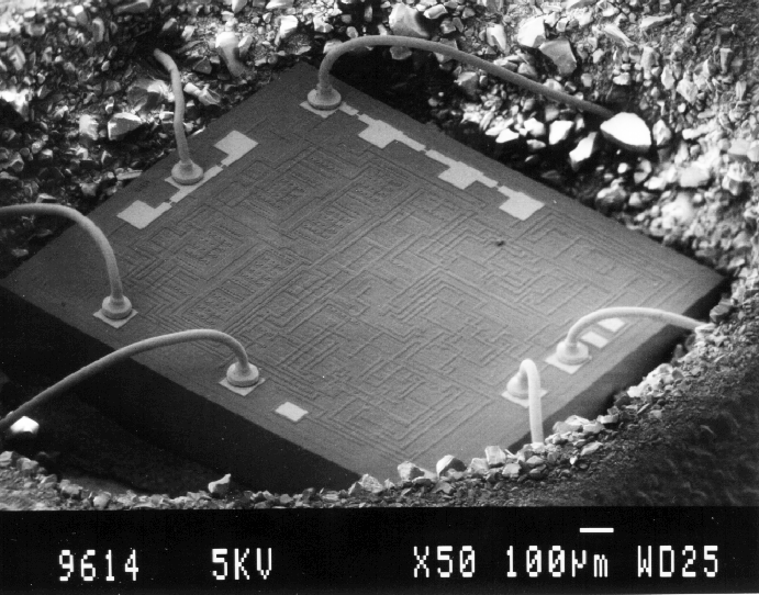
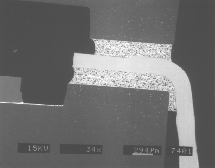
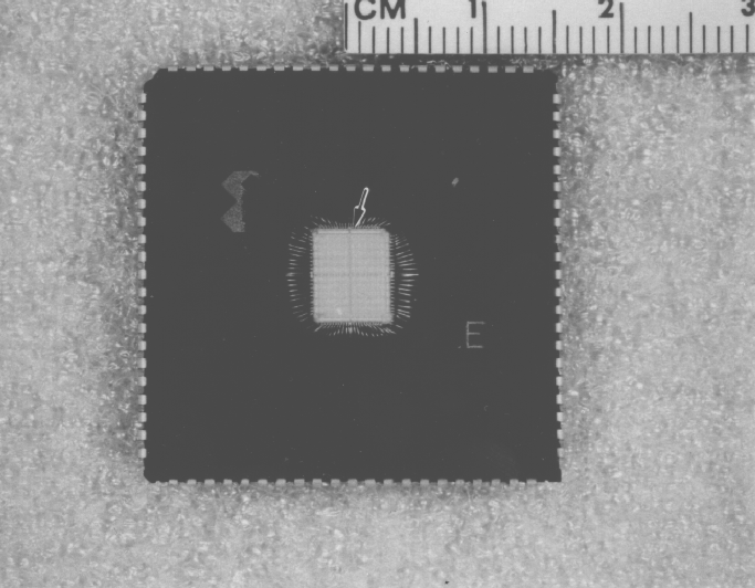
The part is placed into the apparatus according to the vendor's instructions. The stream of acid is started, and hot acid impinges on the surface of the package where the erosion will expose the die. At the end of the cycle, the part is rinsed thoroughly in acetone and examined. The entire process takes a few minutes, and the repeated cycling of the part is minimized (see Figure 5). Figure 6 shows a die that was decapsulated using the jet etch technique. Figure 7 shows a closeup view of a similarly decapsulated package. When the process is complete, the equipment is cleaned, and the waste is disposed of as hazardous waste according to local safety and legal provisions.

Prior to chemical decapsulation by manual techniques, the excess polymer thickness above the surface of the die should be reduced by mechanical milling (preferred, although grinding or sawing may also be used). The most favorable way to do this is to cut a stepped recess that leaves the wirebond loops intact but comes close to the IC surface inboard of the wirebonds on the die. X-ray images or experience with devices will assist in the close approach to the die surface and wirebonds without damage. Removing this material can reduce the chemical etching time and the risk of undesirable etching or tarnishing on the die. The recess also helps localize the acid to the area above the die, sparing the leads and the package body.
In certain cases, it may be acceptable to remove the wirebond loops in order to get close to the surface of the die. The polymer above the die would be ground until the footprint of the wirebonds on the die surface is contacted. Because the interconnect is sacrificed, any subsequent electrical testing would require mechanical probing. This technique may save preparation time and requires less time to etch to the surface of the die.
Note: As with any of the acid etching steps, this method should be performed in a fume hood with proper exhaust and lab practices, including the use of gloves, safety glasses and face shield, and apron.
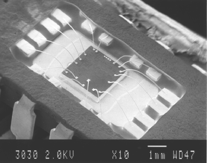
By using a laboratory dropper to apply a small amount of red fuming nitric acid, most of the body of the part and the leads are protected from chemical attack while the die surface is exposed. This method is effective on novolac epoxies, which are most commonly used. The acid will not significantly attack the plastic unless the process is carried out at an elevated temperature. The part is supported on a copper or aluminum heating block which is sized to conduct heat from a hotplate directly to the back of the plastic body of the part. This heating block is placed in a dish which will capture waste acid, and this dish is placed on a hotplate. When the temperature reaches 100oC, a few drops of red fuming nitric acid can be dispensed to the polymer above the die surface, and chemical reaction begins to expose the die. As has already been mentioned, the selective thinning of the polymer above the die will shorten the exposure of the die to acid. After a short time (<30 sec.), the chemical action slows down, and a few more drops can be added. Finally, the part is removed from the block and dipped in red fuming nitric acid at room temperature for a few seconds as a first rinsing step. The part can then be immersed or sprayed with acetone or isopropanol. Water should be avoided as it will result in damage to the metal layers on the integrated circuit. A final ultrasonic clean in methanol followed by drying will permit inspection of the part. Following inspection, it may be necessary to repeat the acid and rinse steps until the die is fully exposed. Following decapsulation, all waste must be properly disposed (see Figure 8).


Note: As with any of the acid etching steps, this method should be performed in a fume hood with proper exhaust and lab practices, including the use of gloves, safety glasses, face shield, and apron.
This technique involves the immersion of the entire device in fuming sulfuric acid. Concentrated sulfuric acid may also be used, but the fuming acid is preferred. The sample preparation with a milled recess may make it possible to expose the die while some mechanical support for the die and leadframe is preserved. A fixture to hold the leads will come in handy if it is necessary to dissolve the entire plastic body. The sulfuric acid must be heated to reduce the amount of moisture which will contact the die. Heating to 150-250oC will decapsulate polymer devices. Following immersion in hot acid for 1 to 2 minutes, the part should be rinsed by immersion in room temperature acid, followed by an immersion rinse in acetone. Inspection at this point will show whether acid steps need to be repeated. Finally, an ultrasonic clean in acetone and drying will complete the process. Following decapsulation, all waste must be properly disposed (see Figure 9).


Decapsulation of polymer packaged devices using plasma is very slow compared to chemical techniques, but it is effective. There is a lower risk of contaminating the part and the electrical function of the part is readily preserved. The prior removal of excess polymer over the die and wirebonds is still recommended. Masking the part so the plasma contacts only this area is also recommended. Etching at high power increases the speed of material removal but decreases the selectivity. The rate of removal can be high initially, but should be decreased as the die surface is approached to protect the chip passivation. In a parallel plate type reactor, the non Reactive Ion Etch (non-RIE) mode should be used. In a barrel reactor, energetic ions are shielded from the sample. The main reactor gas used is oxygen, with initial amounts of CF4 added in the proportion of about 10%. As processing proceeds, the proportion of CF4 should be reduced to about 3%. Reaction products from processing with CF4 are toxic and must be properly vented. The pressure should be maintained in the range of about 750 to 800 mTorr and the power setting is about 200W. After each 1-hour interval in the plasma, the part should be removed from the chamber and the ash that will collect should be dusted away with a clean spray of compressed air. Following inspection, one should determine whether to repeat the process. A total time of six to eight hours can be anticipated.
The procedures listed here for plasma processing have been drawn from the references, where they are proposed as a starting point. A certain amount of experimentation and tuning on non-critical devices can help to ensure success on an actual failure analysis.
Sulfuric acid
Ref. 1 states that when a device is decapsulated in fuming nitric acid (oleum) it should always be quenched (rinsed) with deionized water first. Quenching first in methanol will produce poisonous dimethylene sulfate. After thorough rinsing in deionized water, methanol is recommended.
Ref. 1 doesn't specify any particular rinse or quench for jet etch technique with sulfuric.
Ref. 2 states that water rinse should not be used during decapsulation process with concentrated or fuming sulfuric acid submersion technique. It also states that acetone rinse should not follow hot acid submersion. It recommends acetone after room temperature acid submersion.
Ref. 2 lists acetone and MEK in materials for jet etch technique but procedure doesn't refer to them again.
Nitric acid
Ref. 1 recommends for both the immersion and dropper technique with red fuming nitric, a neutralizing process consisting of a dip in red fuming nitric at room temperature, followed by immersion in isopropanol and ultrasonic cleaning in methanol. No rinse is referred to in the jet etching procedure.
Ref. 2 recommends a rinse in acetone or MEK, then ultrasonic following jet etch with fuming nitric or fuming nitric mixed with sulfuric (doesn't specify fuming or concentrated).
Ref. 2 recommends acetone submersion following dropper technique with red fuming nitric.
Decapsulation should be performed in a sequence which does not compromise the ability to obtain other necessary information from a sample. It is assumed that the packaged integrated circuit has already been removed from its assembly. Decapsulation should follow radiography, external visual examination, leak check, Particle Impact Noise Detection (PIND) tests, Residual Gas Analysis (RGA), or acoustic inspection where it is prudent to perform these analyses.