System Maintenance occurs every Friday.
System Maintenance occurs every Friday.
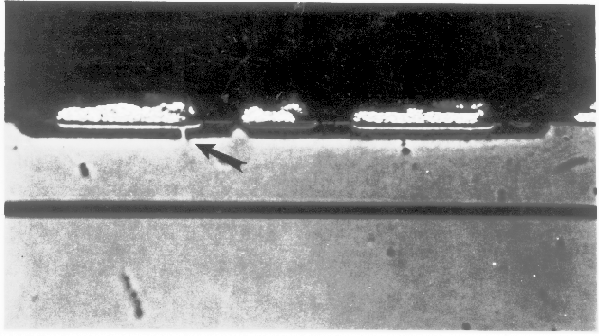
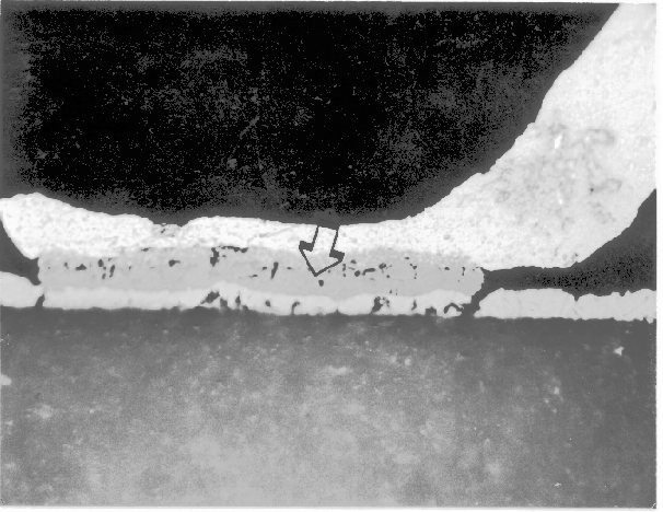
An optical examination after cross sectioning is the examination (with an optical microscope or scanning laser microscope) of cross sectional information exposed by mechanically cross sectioning the IC or wafer or cross sectional information exposed using a focused ion beam. The optical microscope, while not as useful or powerful on cross sections, can nonetheless yield information concerning the processing of the IC, including larger feature sizes, step coverage, etc.
The main reason to perform an optical examination after cross sectioning is lack of access to an SEM. The optical microscope is very useful, however, for tracking progress while you are performing the cross section.
For help on how to operate an optical microscope, consult your operator's manual. To examine a cross sectioned sample, simply place the sample under the microscope and inspect the device. You may want to place fiduciary marks near the area of interest so that you can quickly locate the defect. This is especially important on large memory ICs where the structures are repetitive and difficult to follow. Keep in mind that an optical microscope will not have the resolution necessary to examine smaller features and more advanced technologies.
Perform an optical examination of the cross-sectioned surface immediately after you have finished the cross section.