System Maintenance occurs every Friday.
Light emission is commonly used to mean radiation in the visible wavelength range due to photons emitted by discrete semiconductor devices and ICs. Various defects and failure mechanisms of MOS and bipolar ICs produce photon emission. Normally operating devices will also produce light under certain conditions. The mechanism proposed to explain this photon generation deals with hot carrier production and subsequent energy release. Light emission microscopy refers to technique of utilizing this light to localize and identify defects and failure mechanisms.
Photoemission microscopy has been used for many years for specific analytical purposes and is being increasingly used as a general purpose too for IC failure analysis. The first report of light emission from reverse-biased Si junctions has been attributed to Newman's paper in 1955 [2,3]. The correlation of nonuniform photoemission with silicon dislocations was shown by Chynoweth and Pearson in 1958 [4], who observed that only a small fraction of the dislocation sites emitted light. Other early papers reported the observation of uniform light from defect-free junctions [5] and investigated light emission from microplasma sites [6]. More recently, photon emission has been used to investigate silicon integrated circuit defects such as gate oxide shorts [7-9] and electrostatic discharge damage [9,10]. In addition, photon emission has been used to analyze IC failure mechanisms including latch-up [11,12], snapback [13-15], hot-carrier degradation [16-18], and defect-free structures in "normal" operation including dielectric films [19], MOS transistors [14,15,20], and ICs [16,18].
In order to better understand the nature of the emission spectra from various processes in silicon devices, a general treatment of emission from indirect gap semiconductors is presented.
General recombination processes in semiconductors can be broken down into two main categories: interband and intraband.
Radiative interband transitions occur when an electron in an excited state (occupying a state in the conduction band for example) recombines with a hole (or empty state) in a lower energy band (a hole in the valence band for example) to emit a photon. In indirect gap semiconductors such as silicon, this process must be accompanied by the emission or the absorption of a phonon as illustrated by the energy band diagram in Figure 1(a). Because of the relative lack of phonons for absorption at room temperature, this process is usually dominated by phonon emission. This means that, for indirect materials, there will be significant amount of radiative emission at energies that are a phonon (or a combination of phonons) less than the bandgap or at slightly longer wavelengths. Additional spectral content can come from recombination involving impurity energy levels, both donors (P at E = EC - 0.045 eV and As at E = EC - 0.054 eV) and acceptors (B at E = EV + 0.045 eV) which can further reduce the emitted photon energy and thus push the emission wavelength farther into the IR range as illustrated in Figure 1(b). Hot electrons (or holes) wich carry energy kTe = ?E, represent the only major component by which light at energies significantly greater than the indirect bandgap can be emitted.
![Energy band diagrams for indirect transitions (a) Phonon assisted transitions (b) Impurity and/or hot electron (kT<sub>e</sub> = ΔE) assisted [28].](/reference-material/failure-and-yield-analysis/failure-analysis-die-level/images/light-emission-image-1-medium-2x.png)
![Energy band diagrams for indirect transitions (a) Phonon assisted transitions (b) Impurity and/or hot electron (kT<sub>e</sub> = ΔE) assisted [28].](/reference-material/failure-and-yield-analysis/failure-analysis-die-level/images/light-emission-image-1-small-2x.png)
Intraband recombination, as the name implies, occurs when an excited electron recombines with a vacant state in the same band. Usually, this process will not lead to a photon of significant energy for defect detection purposes but it could conceivably contribute if the energy of the excited electron is more than 1 eV or so above the conduction (or below the valence) band edge. This type of emission is a component in the continuum commonly found in light emission spectra.
Photon emission from defects or abnormal operation of silicon microelectronic devices generally falls into only a few of the possible categories: forward or reverse biased pn junctions, transistors in saturation, latchup, and gate oxide breakdown.
Forward biased pn junctions have perhaps the easiest photon emission mechanism to understand. The mechanism is very similar to that of light emitting diodes (LEDs) and semiconductor lasers. The emission of these devices is generated by placing a large population of electrons and holes in close physical proximity where they recombine. This generates light with spectra centered around the bandgap. Usually, because this is a low voltage emission mechanism, there will be very few highly energetic carriers and thus the photon emission will not extend significantly toward shorter wavelengths. An example of this process found in a very early, but highly referenced article [4], is shown in Figure 2. Figure 2 shows the emission spectra for both forward and reverse (which will be described below) biased pn junctions.


Reverse biased pn junctions represent a different situation. When a small reverse bias is applied to a junction, the depletion region widens, causing low current but a substantial electric field. As the reverse bias is increased, the probability that a highly excited electron will cross the junction increases. This will generate photons from the recombination of carriers whose energies can be significantly above the bandgap energy. The resulting emission spectrum will have a significant tail which can extend into the visible wavelengths. If the reverse bias is increased to the point of avalanche breakdown, the added emission from charge multiplication will dramatically increase the visible photon intensity as well. Although there can be a significant amount of visible light emission, the peak intensity of the emission spectrum will be near the indirect bandgap. The second curve in Figure 2 shows a spectrum of a reverse biased pn junction. Figure 2 shows that even though there is a tail at shorter wavelengths, the NIR emission component has the highest intensity.
A significant group of IC failure modes are the result of MOSFETs in saturation, including certain open and short circuits of metal or polysilicon interconnections. Detection of emission from saturated transistors has been successful for n-channel MOSFETs but difficult for p-channel devices because of their much lower emission intensity.
To understand this emission process, the emission source must be considered. In a MOSFET, a gate voltage above the threshold voltage will create an inversion layer (a conductive channel) between the transistor's source and drain. If the voltage on the drain of the transistor is increased, the depletion layer around the drain will neutralize the inversion layer and pinch off the channel at the drain side. Charge flow between source and drain must now include a drift component as carriers cross the pinchoff region. Evidence has shown that the light emission intensity is strongly coupled to the amount of substrate current. This indicates that the energetic carriers from the source or drain are radiatively recombining with majority carriers from the body of the MOSFET. Because this is similar to the reverse biased pn junction, the spectrum should be similar. Figure 3 shows a spectrum obtained from an n-channel MOSFET in saturation. The similarity to the reverse bias curve in Figure 2 supports this hypothesis. The transistor in Figure 2 was biased with VDS = VGS/2, a situation known to maximize substrate current and photon emission.


While this process creates photons detectable with most commercial light emission systems, light emission from p-channel MOSFETs under the same conditions is more difficult to detect. This is due to ionization potential differences between electrons and holes, making emission from p-channel transistors significantly weaker. For n-channel transistors, as Figure 3 demonstrates, the strongest emission is in the NIR range. Thus, to detect the weaker emission from p-channel transistors and thereby increase defect detection, an NIR detector is the optimal choice.
A third mechanism producing light emission is latchup. The classic model for latchup in CMOS ICs uses two parasitic bipolar transistors connected to form a silicon-controlled rectifier (SCR). When the SCR goes into its "ON" or low impedance state, all three of the SCR junctions are forward biased, placing the bipolar transistors in saturation. For these conditions, the expected emission spectrum will be of the same general shape shown in Figure 2 for a forward biased pn junction. The difference in this case is the relative area occupied by the parasitic SCR in comparison to a single pn junction on the same IC and the resulting amount of current required by the circuit during latchup. These factors make imaging latchup events possible with a silicon CCD camera or an intensified camera by providing more emission at shorter wavelengths, but, at the same time, the NIR intensity is also much larger.
Perhaps the most difficult emission to explain is that of gate oxide shorts. This is a very common failure mechanism that is very difficult to locate without the use of light emission techniques. When gate oxide fails, a conductive path is created through the oxide. This connection is like a local alloy junction between the gate material, usually polycrystalline silicon, and the single crystal silicon in the channel region or in the source/drain region of the transistor. This situation would lead to an expected emission spectrum similar to those shown in Figure 2. As will be shown later, measured spectra indicate that there is a strong component in the visible that decays in the NIR. This might indicate that the emission is thermionic, but the temperature needed to create a visible emission peak makes this unlikely. The exact emission process for gate oxide failures is not well understood.
Several electronic structures have been investigated for light emission properties and the relationship of these properties to their associated currents and bias conditions. These structures include: (1) diodes, (2) n- and p-channel test transistors, (3) a 49 stage ring oscillator, and (4) four ICs that had different types of defects which were localized using photoemission microscopy. The diodes and transistors provide base knowledge of device behavior and the circuit provide a verification of these properties at higher integration levels. All measurements were performed at room temperature.
The diodes were square n+ regions with 1000 µm sides in p-wells. The diodes were evaluated to provide a reference for the analysis of the transistors. The characteristics of the individual n-channel and p-channel test transistors are shown in Table 1. below. All of these transistors had polysilicon gates with no metallization over the gate region. The 1.25 and 1.75 µm transistors were fabricated with a twin-tub process and all others were made with a p-well process. The 1.25 µm n-channel transistors had lightly doped drain (LDD) structures and the other transistors had conventional source/drain regions.
| Channel Length (drawn, µm) | Channel Width (drawn, µm) | Drain Structure | Gate Oxide Thickness (Å) | |
|---|---|---|---|---|
| n-channel | 1.25 | 30 | LDD | 180 |
| 2,3, and 4 | 16 | non-LDD | 450 | |
| p-channel | 1.75 | 30 | non-LDD | 180 |
| 2, 3, and 4 | 16 | non-LDD | 450 |
Two ring oscillators, each having 49 inverters, have been evaluated. The n-channel and p-channel transistor width/length dimensions were 5/1.25 and 5/1.5 µm for the first oscillator and 20/1.5 and 28/1.75 µm for the second oscillator; the n-channel transistors had LDD and the p-channels were non-LDD structures. These oscillators were tested at VDD = 5 V and at this voltage the self-oscillation frequencies ranged from about 25 to 35 MHz.
The diodes were analyzed in the reverse bias condition. Light emission was observed in real time (without signal integration) as the magnitude of the reverse bias voltage was increased from 0 to 20 V. Avalanche breakdown of the diode occurred at about 19 V and light was not observed until the bias reached this magnitude. Initially, light spots formed at the corners of the diode structure; this location of emission is consistent with the higher electric fields that occur at the corners. Faint light emission with no signal integration was observed at one junction corner with diode current as low as 25 µA. As the reverse bias voltage was increased, a continuous ring of light formed at the edges of the structure. Although these diodes had no evidence of point defects, it is common to observe light emission from random locations around the junction periphery which corresponds to the pre-avalanche leakage current characteristic of "soft", defective pn junctions.
Light emission of the reverse biased drain to p-well junction of an n-channel test transistor (3 µm channel length) was also observed in real time as the reverse bias voltage was swept beyond the junction breakdown voltage. Initially light spots appeared at the outer corners of the drain junction boundary and then emission increased to a continuous line of light along the drain as the bias was increased.
The light emitting properties of the four different types of n-channel test transistors were measured. The light emission amplitude and associated drain and p-well currents were observed as a function of gate-source and drain-source bias voltages. Identical bias voltages, current measurements, and light emission amplitude measurement techniques were used for all four types of n-channel transistors. The differing transistor geometries were chosen to observe the light emission properties as the channel electric field strength was increased with decreasing channel length and constant VDS.
The magnitude of the light emission for a given transistor was measured and was found to correlate with the magnitude of its p-well current (IPW), an observation attributed first to Childs et al. [27] and subsequently reported by others [14,16,23,28]. The drain current (ID) and IPW magnitudes are given in Figure 4 for the 2 µm channel length transistor with VDS = 5 V as VGS was swept from 0-6 V. Figure 2 shows that the peak of IPW occurs at approximately VDS/2 while ID continues to increase as VGS increases. Light emission was observed for ID values as low as 500 nA.


Figure 5 shows a normalized plot of light emission intensity data as a function of VGS (VDS = 5 V). The shape of this curve is similar to that seen in Figure 4for IPW, which is normalized and replotted in Figure 5. The approximate correlation between light emission amplitude and IPW can be seen in the two curves. An important observation is that significant light emission is found only in a restricted region of the saturated state of the transistor. Normal logic states (and some logic voltages produced by defects) cause transistors to be in a non-saturated bias condition and therefore to emit relatively low intensity light.


In Figure 6, the light emission amplitude for three different channel length transistors is plotted as a function of VGS (VDS = 5 V) and transistor channel length with the light emission normalized to that of the 2 µm transistor. The large increase in light emission observed for decreasing channel length (and hence increasing channel electric field strength) is apparent.


Currents and voltages (ID, ISUB, VGS, VDS) of the 2, 3, and 4 µm channel length p-channel test transistors were measured in a manner similar to that of the n-channel transistors. Light emission was not observable in any of the p-channel transistors at VDS = - 5 V with VGS = - 2.5 V using the EMMI maximum integration time of 2000 frames. VDS was then increased to a maximum of - 10 V for the substrate current and light emission measurements of the 2, 3, and 4 µm channel length transistors. The substrate current was measured at VDS = - 5 V for the 1.75 µm transistor. The much lower light emission associated with p-channel devices made higher drain voltage biasing necessary. Figure 7 shows ISUB and ID as functions of VGS for a 2 µm transistor with VDS = - 10 V.


For comparison Figure 8 shows IPW and ID for a 2 µm n-channel transistor as a function of VGS at VDS = 10 V. Figs. 7 and 8 show approximately similar p- and n-channel transistors characteristics for their respective substrate and p-well photon-induced currents. The n-channel peak current was IPW = 246 µA and the p-channel peak current was ISUB = 14.3 nA. The ratio is about 17,000 and is an approximation of their respective light emission intensities under the same biasing conditions. Direct comparison of the photoemission amplitude over a 17,000X range is beyond the dynamic range capability (2000X) of the EMMI, so only a comparison of ISUB and IPW is possible.


The magnitude of the light emission for the 2 µm channel length p-channel transistor again approximately correlated with the magnitude of the substrate current. Figure 7 shows that the peak of ISUB occurs at approximately VDS/2 while ID continued to increase as VGS increases. Figure 9 shows the normalized comparison of the integrated light emission signal and the normalized substrate current. As with the n-channel comparison, an approximate correlation is observed.


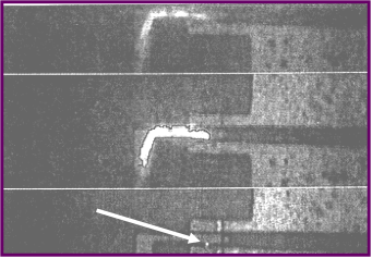
Several non-defective n-channel transistors were biased with a ramp voltage on the gate to p-well regions. At approximately 55 V, the transistor gate oxide ruptured. This formation of a gate oxide short was observed as a bright flash of light. The flash event was captured by videotaping the output of the EMMI during gate oxide rupture and then digitizing the video frame-by-frame (Figure 10). This flash was interpreted as possible photoemission by energetic surface carriers due to current crowding (skin effect) on the surface of the conductor [29]. This current crowding may be due to high instantaneous current of capacitive discharge during the rupture event [30]. The duration of the light flash was probably much less than the video frame time (33 ms), but the saturation and slow response time of the photoemission system facilitated its observation. Note that the light flash bends towards the inner corner of the metallization where the electric field is concentrated and ends at a point on the transistor gate. This "end" point is the physical location of the gate oxide short. This phenomena was observed on several other gate oxide rupture experiments, including p-channel transistors.
Ring oscillators were used to demonstrate that light emission could be observed for transient switching situations. Each transistor in the ring emits light when it is saturated during the logic transition. The ring oscillator was allowed to operate while the EMMI performed a 300 frame integration of the light emission from the surface of the circuit. The oscillator frequency was about 30 MHz for VDD = 5 V.
Figure 11 shows the light emission from n-channel transistors of the ring oscillator. The light emission that occurs during the transition is individually too weak to detect for a single cycle, but over the course of many millions of cycles, light is detected in the 1.25 µm n-channel transistors of this circuit. It was not possible to observe emission from the 1.5 µm p-channel transistors of this circuit, which is consistent with the individual transistor emission characteristics described previously. This capability of photoemission microscopy to detect transient light events that would not yield sufficient emission in the static bias condition is useful for many CMOS circuits and for dynamic MOS circuits.
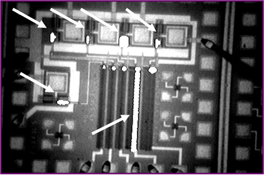
Figure 12 shows a transistor schematic for a conventional, static CMOS inverter. Figure 13 shows the logic transfer and measured IDD characteristics for this type of inverter. This inverter was made from one of each of the 2 µm channel length (16 µm channel width) n and p-channel transistors. For these measurements inverter input VG varied from 0 to 5 V with VDD = 5 V. The points where VGS is approximately VDS/2 for the n and p-channel transistors are shown on this figure as "N-CH" and "P-CH", respectively. These values are near VGS = 1.9 V for the n-channel transistor and VGS = - 2.4 V for the p-channel transistor (VG = 1.9 and 2.6 volts respectively).


Figure 14 shows the n-channel p-well (IPW) and p-channel substrate (ISUB) currents for the same inverter of Figure 13. Note that the peaks of IPW and ISUB are within about 0.4 V of the VGS = VDS/2 points and that the peak of ISUB occurs at nearly the same value of VG as the peak of IDD.


The photon emission for the n-channel transistor TN will follow the IPW curve and will occur over an approximate range of 1.0 V < VG < 2.0 V, with peak intensity at about VG = 1.6 V. It is significant for failure analysis to note that there is a region from 2.0 < VG < 3.6 V (Figure 12, 13) in which elevated drain current exists, but IPW and photon emission are absent. The p-channel does not emit significantly during the inverter transition as evidenced by the very small ISUB peak of about 200 pA.
Four cases are given from failure analysis performed at Sandia. These examples were chosen to illustrate the use of photoemission analysis to identify and localize physical defects in CMOS ICs.
Case 1: This IC was designed and manufactured by an ASIC vendor using a gate array technology with 1.5 µm transistor channel lengths (drawn). The IC performs a custom logic function with about 8100 logic gates. The photoemission analysis located multiple gate oxide shorts (Figure 15).

These light emitting gate shorts were observable simply by repeatedly applying power to the IC and observing the "random" power-up logic state (no input stimulus changes were applied after power-up). It was possible to change the power-up logic state (and therefore the gate oxide short bias/photoemission) by changing the microscope background illumination intensity during the power-up. The changes in the illumination produced variation in the power-up logic state due to the injected photocurrent effect on logic gate stabilization. For this case it was not necessary to utilize complex digital test equipment for the IC stimulus in order to successfully achieve photoemission for defect identification. This fortuitous occurrence of photoemission without the application of complex IC stimuli has often happened during failure analysis at Sandia, justifying the use of simple power-up and initialization/clocking techniques prior to the use of more complicated stimulus conditions. For these situations, it appears that defects can preferentially influence the power-up conditions so as to result in the most favorable logic (bias) condition for light emission. In some cases, however, it has been found to be necessary to utilize large digital test equipment to provide over 10,000 test vectors to the IC to produce the light emitting condition.
A different fabrication version of this IC had a parasitic n-channel transistor problem. Although these parasitic transistors were operating in a saturated bias condition (VG = VD = VDD =10 V), no light emission was observable with the KLA EMMI system. This occurred because the effective channel length for the parasitic transistors was very high (about 30 µm) producing a very low drain/p-well electric field. (ID for each parasitic transistor was about 20 µA).
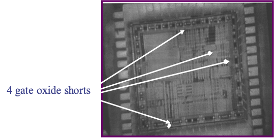
Case 2: A 16/32-bit microprocessor equivalent to the National 32C016 (about 65,000 transistors; 1.25 µm technology) had gate oxide shorts that could not be determined from random power-up logic conditions. A 15K test vector set was then cycled repeatedly through the IC while the EMMI was put in the integration mode. Four transistors having gate oxide shorts were detected (Figure 16). This case illustrates that the integration mode of the EMMI can be used to find defects, again without identification of the specific test vectors responsible for producing light emission.
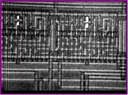
Case 3: A functionally-failing 2-channel scaler IC of about 2000 transistors did not produce light emission for a normal application of vectors. However, it was noticed that the quiescent power supply current (IDDQ) spiked for about 0.25 seconds during power-up. The EMMI was put in the integration mode and the IC was repeatedly powered up. Several n-channel transistors showed light emission in a row of flip-flops (Figure 17). Upon further inspection, these transistors were found to not be defective, but were being driven by a clock line that had a metallization open circuit. The clock line provided the clock signal input to the flip-flops. The light emitting n-channel transistors were in the inverters which were the first gates connected to the clock input inside the flip-flops. This case illustrates another type of failure analysis situation in which the light emitting devices may not be defective, but their emission is a result of a defect or failure mechanism in the electrical (nodal) vicinity.
Case 4: This IC is a custom interface controller with about 8000 transistors (2000 logic gates) and was manufactured using the same technology as the IC of Case 3 (Sandia's 4/3 technology: 4 µm minimum width metal and 3 µm minimum width polysilicon [6]). This IC failed due to a photoresist defect which produced a metallization patterning error that shorted the output of a 2-NAND to VDD. Photoemission was observed in one of the n-channel transistors of this logic gate (IDS for both 2-NAND n-channel transistors in series was about 4 mA at VDD =5 V). The reason for light emission from only one of the two n-channel transistors will be discussed in the next section.
Photoemission microscopy is a powerful tool for CMOS failure analysis. In certain cases, small submicron defects or failure mechanisms can be identified within minutes of equipment setup with this nondestructive analysis technique. This technique is particularly useful in quickly locating certain defects, such as "soft" pn junctions and gate oxide shorts. The electrical stimuli (test vectors) required to expose these particular defects can often be the random states associated with power-up of the IC. For very low level defect light emission, continuous cycling of the IC over many millions of test vectors can identify the defect using the photoemission microscope integration mode. The location of non-light-emitting defects by identification of hot electron photoemission in transistors driving the defect is less straightforward but can also be very effective. The data presented here and by others show that light emission will not occur unless the drive transistor has terminal voltages that place it into a saturated bias state. The saturated bias state is defined as the region where VDS > VGS - VT and VGS > VT (VT = threshold voltage). A high electric field in the channel is a necessary requirement for transistor photoemission. The magnitude of the drain current is not directly correlated with this photoemission.
Several factors may increase the hot carrier light emission for a particular transistor: (1) enhanced AC biasing effects, (2) circuit design, and (3) statistical variation due to fabrication. It has been observed that, under certain conditions, hot carrier degradation during AC operation may be increased over DC biasing degradation [32-34]. Such AC degradation increases with increasing clock frequency and can occur in transfer gates in static RAM cells [34]. Although some of the enhancement may be due to experimental setup [35], the possibility of enhanced degradation was not conclusively eliminated. In fact, in a CMOS static RAM, the access transistor degradation was found to be the limiting hot carrier concern for the IC [17]. These access transistors were found to emit more light than surrounding transistors.
Certain areas of a circuit may be more susceptible to hot carrier stress than others. The transfer gate mentioned above is one example. It is also possible that certain transistors may be weaker due to statistical fabrication variations within the transistors [36]. These transistors may see the same bias stress as other transistors but degrade more (and emit more photons) due to normal processing variations in such physical parameters as gate oxide thickness and effective channel length.
Two photoemission situations are shown in Figure 18 (a,b), illustrating how high channel current can exist but light emission may or may not be observable. The "worst case" defect (but "best case" for light emission) in Figure 18 (a,b) is a zero ohm bridge (RDEF = 0 O) between the gate output and VDD. In Figure 18 (a) the terminal bias voltages for TN are VGS = VDS = 5 V, therefore TN is in weak saturation. Light will be observed in the drain/channel region of TN although it is not the optimal emission condition. Light would probably not be observed in TP if the defect was a zero ohm connection to the ground bus. TP would be in weak saturation, but its greatly reduced light emission would probably not produce observable photons.


Figure 18 (b) shows a VDD-bridged defect on the output of a 2-NAND gate. When VA = VB = 5 V, a relatively large drain current exists in TNA and TNB. In IC Case 4, this current was about 4 mA for a metallization short to VDD (RDEF = 0 O). For this case, VC = 5 V, VDS = 4 V for TNA and VDS = 1 V for TNB, which resulted in light emission for TNA (saturation bias) and no light emission for TNB (non-saturation bias).
When RDEF is not 0 O, then the VDS values across the affected transistors will depend upon the value of RDEF. In Figure 18 (a), VDS on TN will drop as RDEF increases. When VGS > VDS + VT occurs, TN goes into the non-saturated state and channel light emission ceases.
Therefore, the existence of light emission in a transistor driving a resistive defect load (RDEF > 0) is determined by individual defect resistance values.
Defects that are bridged to power supply voltages can also affect downstream (or driven) logic gates. Figure 19 shows an inverter pair in which a resistive defect is connected between node B and the VDD supply. If VA = 5 V, then VB may not be pulled down all the way to ground voltage. If VB is pulled down to 1 V < VB < 4V (for VT = 1 V), then both transistors of G2 are on and elevated drain current exists in TN2 and TP2. The best case for G2 light emission occurs near VB = 0.5 VC, which depends upon the value of RDEF. If RDEF is large (>10 KO for typical technologies), then TN1 will pull down into non-saturation producing a weak logic zero on node B. This would decrease the likelihood of photo detection. This illustrates that photo detection in G2 may or may not occur depending upon the value of RDEF.


The conclusion for photodetection in driving load transistors is that the bias state and terminal voltage magnitudes are clearly the dominant factors that determine photon emission and not the magnitude of the drain current (or IDD for the IC).
Another powerful detection capability of photoemission microscopy was illustrated in two of the IC failure analysis cases presented here. A defect may cause weak intensity photon emission that is undetectable in a single short cycle of a test vector set. However, continuous cycling of the IC through its complete (or appropriate subset) vector pattern can often expose the defect or failure mechanism if the photoemission microscope is used in an integration mode. This was illustrated in Case 2. Failure analysis in Case 3 uses the same principle, but used repeated power-up cycles. In both of these cases, the defects were detected without knowledge of the relationship between defect characteristics and the specific logic states required for photoemission detection. The success of the photoemission integration technique depends on the rate (duty factor) with which the photo emitting site is biased into its emitting state by the test vector pattern.
Photoemission microscopy, combined with IDDQ testing [37,38], is also a very useful technique for IC design characterization and validation. For example, photoemission from n-channel transistors in an internal memory array of a custom IC was used to determine that high IDDQ after power-up was due to bit lines not initialized or latched properly. Photoemission has also been used in dynamic CMOS circuitry to determine which precharged bit lines in memory arrays discharge first.
Because of the recent popularity of flip-chip technologies and the rapid escalation in the number of metal interconnect layers which obscure the frontside view of transistors, the need for light emission technology for backside (through the silicon substrate) analysis has increased. As the previous sections indicate, there are strong signals from all of the main light emitting defect types in the NIR. To meet this need, both a sensitive detector and one with good quantum efficiency for wavelengths beyond 1 µm is needed.
In order to provide a basis for comparison, the above samples were first studied using a non-intensified silicon CCD camera. The camera used was a liquid nitrogen-cooled, slow-scan camera with a thinned, back illuminated 512 by 512 pixel CCD array. The use of liquid nitrogen cooling effectively reduces the dark current noise to a negligible level, about two electrons per hour. The quantum efficiency (a measure of the detector's ability to collect light at a given wavelength) of this CCD array is shown in Figure 20. Figure 20 indicates that the peak in quantum efficiency is in the 600-700 nm wavelength band with a gradual drop in efficiency with increasing wavelength out to 1 µm. At 1 µm, the detector has a quantum efficiency of 17%. For longer wavelengths, the quantum efficiency drops quickly to only a few percent. The abrupt loss in quantum efficiency near the indirect bandgap of silicon is a direct consequence of the materials used to make the CCD array and demonstrates that silicon detectors may not be the best choice for imaging emission processes in silicon ICs. Although detectors of this type have been marketed in systems for backside light emission analysis, their low efficiency for wavelengths to which silicon is transparent severely limits what can be detected


For comparison to the CCD array specifications, Figure 21 shows the peak radiant sensitivity of several common image intensifiers [15] as a function of wavelength. Figure 21 shows that even the GEN III - NIR intensifier will have limited applicability for the detection of light at energies near the silicon bandgap. These detectors rely on their ability to detect the relatively small amount of light in their spectral range of sensitivity.
![Spectral response of various image intensifiers [15].](/reference-material/failure-and-yield-analysis/failure-analysis-die-level/images/light-emission-image-21-medium-2x.png)
![Spectral response of various image intensifiers [15].](/reference-material/failure-and-yield-analysis/failure-analysis-die-level/images/light-emission-image-21-small-2x.png)
The first samples analyzed with the cooled, silicon CCD array were those with gate oxide shorts. These samples had shorts in both p- and n-channel MOSFETs that were imaged at wavelengths from 400 to 1100 nm using a series of bandpass filters. Once the signal was extracted from the background noise, it was corrected for both the filter response and the CCD quantum efficiency. The typical exposure times needed to achieve sufficient signal-to-noise levels for each image ranged from as short as 5 seconds at wavelengths around 700 nm to over 300 seconds at 1100 nm. Since the sample was fabricated in an 11 V technology, a supply voltage of 11 V was used, resulting in an IDDQ of 6.6 mA. The p- and n-channel gate short samples represent very strong emission sources. The resulting spectra are shown in Figure 22. The data obtained is interesting because there is virtually no difference between the emission spectra for gate oxide shorts in p- and n-channel MOSFETs. This analysis suggests that the emission process is independent of the type of single crystal material to which contact has been made and indicates hot electron processes are responsible for the peak at visible wavelengths. A simple calculation using Wein's displacement law gives a corresponding temperature for a thermionic emission process of over 4800 K, which is clearly not physically possible for silicon ICs. Therefore the emission process must be dominated by electrons which have been excited to well above the conduction band edge radiatively recombining with vacant states in the valence band.


The other process which was characterized using the CCD array was saturation current emission from n- and p-channel MOSFETs. For this test, several 0.5 and 0.6 µm channel length test transistors were biased with VDS = 3.3 V and VGS = 1.65 V in order to maximize the substrate current and thus maximize the light emission. The transistors were imaged using the same bandpass filters as were used for the gate oxide short samples. While the n-channel transistors were easily imaged using an integration time of 300 seconds, emission from the p-channel devices was so weak that no signal could be detected even after 1800 seconds of integration time. Figure 23 shows the spectra obtained from n-channel devices of two different channel lengths and with two different microscope objectives. The differences detected between the two objectives used indicate that the transmission of most microscope objectives is lower near 1000 nm and the quantum efficiency of the CCD array at the same wavelength may be optimistic. The objective used for comparison (Ealing IR lens) was an infrared optimized reflecting objective with a 97% transmission efficiency between 0.95 µm and 10 µm and thus was not responsible for any additional transmission loss in the NIR.
For failure analysis applications bandpass filters normally are not used. Emission detection is normally done using the full spectral width of the detector to minimize integration time. Figure 24 shows the imaging results from an n-channel MOSFET in saturation after 300 seconds integration time and Figure 25 shows the corresponding p-channel images. Both emission images were taken using the full spectral range of the CCD camera system.
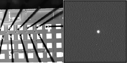
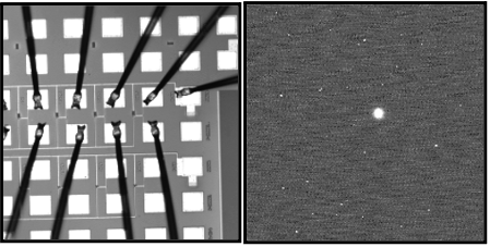
For gate oxide short-related emission, images can be obtained in a matter of a few seconds. As was illustrated in Figure 22, the peak in the spectra related to this particular emission type falls well within the high quantum efficiency wavelength range of CCD arrays. This makes gate oxide shorts easy to detect with visible wavelength detectors.
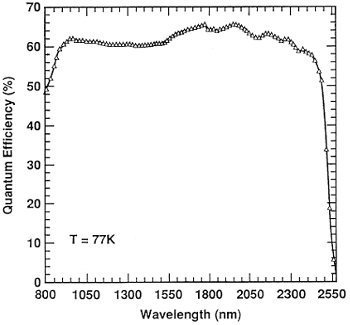
A 256x256 pixel HgCdTe NIR array developed for use on the Hubble Space Telescope was used to image in the 800 - 2500 nm band. This so called NICMOS-3 array was developed for NASA by Rockwell International and the Steward Observatory at the University of Arizona. The overall quantum efficiency of the system is listed in Table 2.
| Wavelength (µm) | Quantum Efficiency (%) |
|---|---|
| 0.8 | cut-on |
| 1.3 | 35 |
| 1.65 | 45 |
| 2.2 | 85 |
| 2.5 | cut-off |
The first prototype camera [16] developed for microscopic applications, now in use at The National University of Singapore (NUS), was designed to utilize the full spectral range of the detector from 800 to 2500 nm. This camera used a cooled, anti-reflection coated ZnSe window to provide good transmission between 500 nm and 5000 nm as well as low thermal emission. This camera incorporates a six position filter wheel cooled to 77 K and incorporates five wide bandpass filters whose center wavelengths and peak transmissions are listed in Table 3. This camera is mounted on a three axis Alessi probe station. This is believed to be the first IR microscope to utilize an NIR array with performance comparable to that of cooled CCD arrays.
| Center wavelength, ?p (nm) | Transmission at ?p (%) |
|---|---|
| 870 | 85 |
| 1100 | 60 |
| 1250 | 60 |
| 1650 | 60 |
| 2200 | 60 |
The usual read noise of the NICMOS-3 array is 35 electrons but modifications using special read techniques can reduce this noise to less than 15 electrons. Because the temperature of the array is maintained near 77 K, the dark current is negligible for integration times from 100 milliseconds to greater than 100 seconds. Thus, it is possible to measure photon fluxes at the array of less than 1 photon per second. While experimental evidence suggests that the emission from IC related processes is still strong past 1400 nm, thermal background from the sample starts to become noticeable and limits the sensitivity to non-thermal emission. In order to eliminate thermal information, a cold filter which has a cutoff at 1400 nm and very low leakage at longer wavelengths can be placed in front of the array. The spectral response of this filter, which is referred to as a J-filter in astronomy, is shown in Figure 26. Except where noted, this camera was used to perform the NIR light emission analysis below.


From both the theory of light emission and the results presented for the Si CCD array camera, the light emission from the most common IC defects should be greater in the infrared than in the visible to near IR range (except possibly for the emission from gate oxide failures). To prove this point, the same samples analyzed with the Si CCD camera were analyzed with the NICMOS camera.
As was done with the CCD camera, both n- and p-channel MOSFETs were imaged in saturation. Both transistor types were biased at VDS = 3.3 V, VGS = 1.65 V which gave a nominal drain to source current of 1.94 mA for the n-channel and 1.2 mA for the p-channel transistors. In contrast to the CCD analysis, the emission from the p-channel transistors was strong enough to obtain high signal-to-noise data with a reasonable integration time. In fact, using the full 1.1 - 1.4 µm wavelength band of the J-filter, emission images could be acquired with less than 10 seconds integration time using the 0.5 µm channel length n- and p-channel transistors. For the spectral work where bandpass filters were placed in front of the J-filter, a 10 second integration time was used for the n-channel devices while a 30 second integration time was used for the p-channel devices. The results, which have been corrected for filter transmission, exposure time, and device current, are shown in Figure 27. As expected, the emission from the n-channel transistors is significantly stronger at all wavelengths, but the p-channel spectrum does maintain the same general characteristics. Both curves have a strong signal at 1.1 µm and a peak at around 1.3 µm (which is harder to see for the p-channel devices because of the vertical scale in the figure). The signal at 1.1 µm is undoubtedly from radiative recombination around the indirect bandgap of silicon. Because the spectra were obtained using discrete filters, no information about the peak width was available. For comparison, Figure 28 shows the results obtained using the NICMOS camera at NUS over the wavelength range from 1.2 to 2.5 µm. The curves in Figure 13 do not show a short wavelength rise indicating that the observed signal at 1.1 µm in Figure 12 may be fairly narrow. It also should be noted that the presence of a strong signal at 1.1 µm contradicts the CCD camera results which indicated a drop in intensity. This contradiction is most likely due to an overestimation of the quantum efficiency of the CCD array even at 1.0 µm.


Since the signals were strong from both transistor types, data was also collected to measure the changes in signal intensity as a function of channel length (and thus electric field). As before, all transistors were biased at VDS = 3.3 V, VGS = 1.65 V. Figure 29 shows the results of this analysis with no bandpass filters in the camera, only the J-filter. As expected, the data shows that the intensity of the light emission from saturation is inversely proportional to channel length.


The SRAM subjected to human body model ESD testing was also analyzed in the infrared. The example I/O structure showed evidence of a leaky protection diode (pn junction) after the ESD testing. With the IC biased at VDD = 3.3 V, it drew a supply current of 5.23 mA. Emission from the damaged input was strong at 100 seconds integration time and was still detectable at 30 seconds. Since emission from this sample could also be detected in a commercial light emission system using an S1 type image intensifier in approximately 10 seconds, some of the damage to the sample may be gate oxide related.
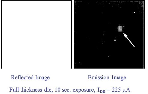
Light emission analysis from the die backside is perhaps the application where infrared cameras are unchallenged by other imaging technologies. To demonstrate this, the backside sample described earlier was analyzed. Figure 30 shows both a reflected infrared image and the corresponding light emission image. The emission in this case was generated by placing one of the output buffer transistors in saturation by applying a voltage of 3.5 V to the output pin. This situation puts both the n-channel and the p-channel output buffer transistors into saturation since for both transistors, VDS > (VGS - VT). A power supply current of 225 µA at a voltage of 5.0 V was measured. The emission image in Figure 30 was made using an exposure time of 10 seconds. Emission images were made with exposure times as short as 1.5 seconds.
The other important feature of this analysis is that no thinning of the substrate was required to reduce absorption. The sample was polished only enough to remove the eutectic die attach and create a smooth interface.
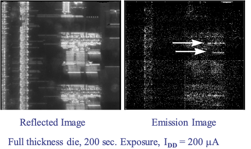
The real challenge was to determine if there was enough emission from the defect area on this sample to be detected. As was found in an earlier study [10], the pellicle scratch created a problem with several contacts. The poorly defined contacts created a situation where several transistors could be placed in saturation. Figure 31 shows both the defect area and the light emission collected after a 200 second integration time. The sample was biased at VDD = 5.0 V yielding a current of 200 µA with the defect state active. It should be noted that the emission from this sample could not be detected with either a commercial light emission system with an S1 type image intensifier or the cooled CCD camera.
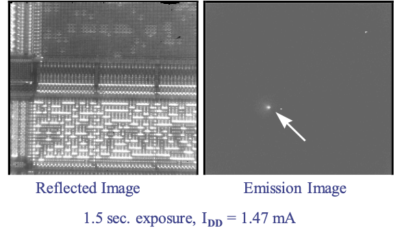
The final series of samples analyzed were those with gate oxide shorts. As shown in Figure 6, the emission from this class of defects exhibited a peak around 600 nm. This finding did create some concern about the potential for imaging their emission in the infrared. As it turned out, all concerns were premature as the emission was easily collected using very short exposure times (less than 1.5 seconds) using the NICMOS camera. Figure 32 shows an example image collected using the full J-filter bandwidth with the sample biased at VDD = 6.0 V and IDD = 1.47 mA (remembering that this sample was manufactured for use at 11 V). While the spectral information shown in Figure 22 for this same sample does contain a short wavelength peak, it is apparent that there is also a strong signal in the infrared, most likely at 1.1 µm, which is easily detected by the infrared camera. This data shows that the gate oxide short class of defects is by far the easiest to detect.
The accurate diagnosis and precise location of failure mechanisms and defects in CMOS ICs are often difficult tasks. Many techniques are available, but successful failure analysis requires careful selection of these techniques and the sequencing of their use. Nondestructive techniques are usually preferred if they are easy to implement and have a high probability of success. Light emission microscopy has several desirable attributes, including high spatial sensitivity, simple sample preparation and installation, and absence of special environmental requirements.