System Maintenance occurs every Friday.
System Maintenance occurs every Friday.
Capacitive Coupled Voltage Contrast (CCVC) is a low primary beam energy scanning electron microscopy (SEM) technique that permits imaging and measurement of dynamic voltages beneath passivation layers. Analyzing the variations in secondary electron image brightness with applied vectors enables measurement of the logic levels of a digital integrated circuit and the voltage of internal test nodes. Using a secondary electron energy spectrometer makes quantitative voltage measurement possible by measuring the energy distribution of the secondary electrons escaping the surface. (Quantitative voltage measurement using CCVC is covered fully in the dynamic voltage contrast help file.) The major advantage of CCVC over static voltage contrast is the elimination of irradiation damage when examining passivated ICs. In addition to the lack of irradiation damage, since CCVC of passivated ICs only displays the structures with changing voltages and not static voltages, CCVC images are easier to examine than static voltage contrast images.
CCVC measures the changing logic level (voltage) of a passivated conductor on an IC. CCVC can verify the functionality of an internal IC logic gate by observing dynamic input and output logic states of the conductors associated with the logic gate. CCVC can also verify the continuity of a conductor by examining the secondary electron contrast along the length of the conductor when dynamic voltages are supplied. An abrupt change in the CCVC signal intensity along a conductor could indicate an open conductor.
In CCVC, the logic state of the conductor can only be observed when changing from one state to another; therefore, some means of changing the voltage of the internal conductor is required.
To understand how CCVC is performed, this section will explain voltage contrast (VC) and CCVC.
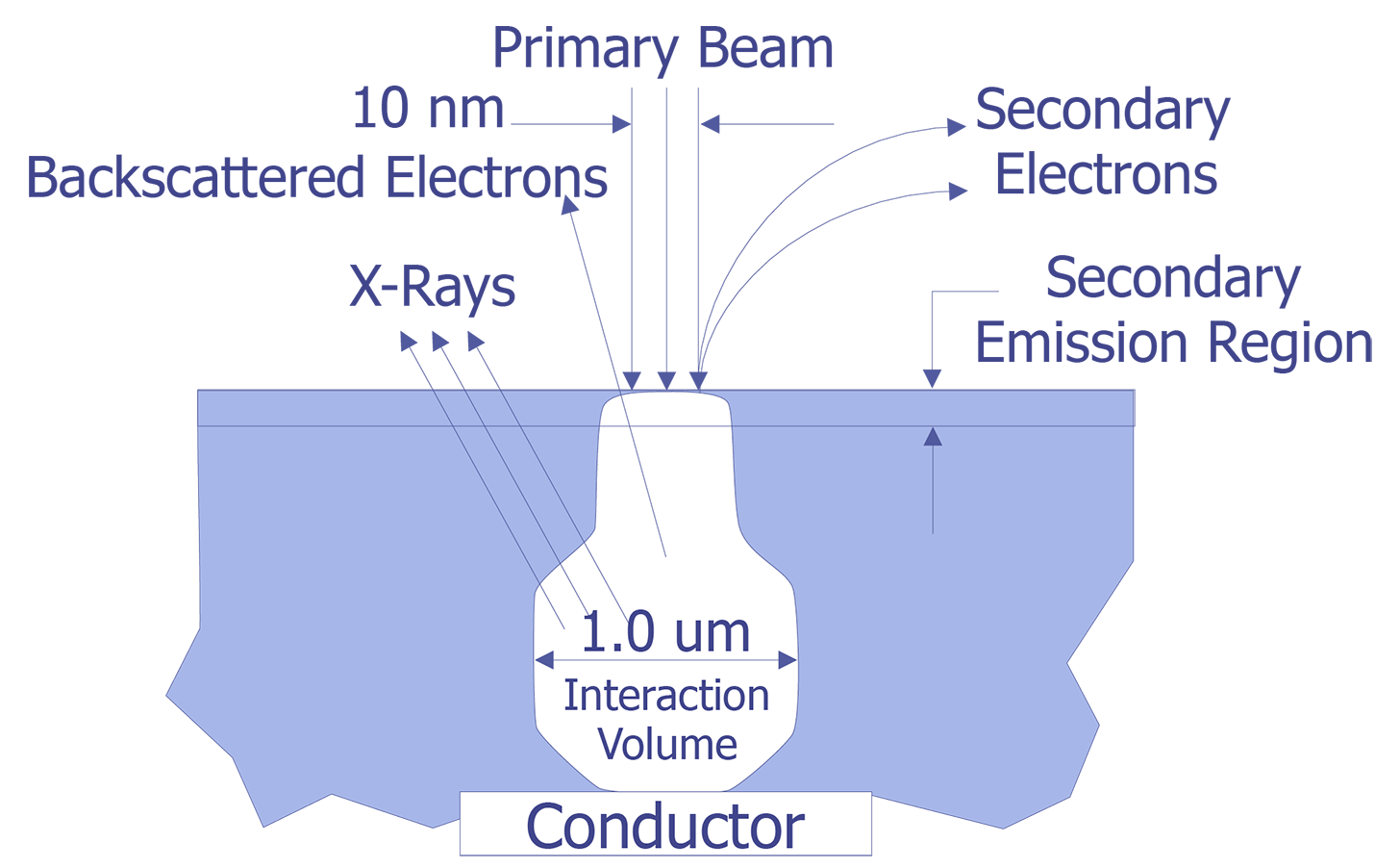
VC imaging takes advantage of differing secondary electron emission efficiencies with applied bias on ICs. Figure 1 displays the electron beam interaction products between silicon and a 10 keV primary electron beam . Secondary electrons are defined as those electrons emitted from the surface with energies of 50 eV or less after primary electron beam exposure. The complex theory behind secondary electron emission involves secondary electron generation, transport to the surface, and escape from the surface. The typical shape of the secondary electron energy distribution is shown in Figure 2 . Because of their low energies, secondary electrons are generated only from about 30 nm or less from the surface. The ratio of the electron flux escaping the surface of an exposed device to the electron flux injected into a sample varies with the material examined and the primary electron beam energy used. For microelectronic materials at relatively low beam energies (<2 keV), more electrons escape from the surface than are injected. At higher energies, fewer electron escape than are injected. Under both conditions, the surface has a net charge. For the case of low beam energies, a positive charge builds up on the surface. This charge will prevent lower energy secondary electrons from escaping the surface and a positive equilibrium voltage (about 0.5 V with a 1.0 keV beam) will be established at which the escaping and incident electron flux are equal.


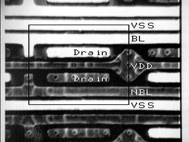
If the surface of the target can be forced externally to a different voltage locally, then the secondary electron image will have increased or reduced signal depending upon the difference between the forced voltage and the equilibrium voltage. The conductors of a depassivated integrated circuit may be forced in such a manner, resulting in the image shown in Figure 1.
CCVC uses the passivation layer as a discharging capacitor to generate a dynamic image of changing subsurface voltages. CCVC is performed at fast electron beam scan rates (~TV rates) to increase the time resolution of the dynamic signal. As desrcibed above, at low primary electron beam energies (<2 keV), more electrons escape than are injected by the primary electron beam. A net positive charge will build up on the surface, preventing lower energy secondary electrons from escaping the surface and decreasing the secondary electron image intensity. An equilibrium voltage is reached when the net charge accumulated on the IC does not change with time.
A bound surface charge will be produced when structures below the maximum beam penetration depth change potential, and the material between them and the surface becomes polarized. The CCVC signal is the temporary change in the number of secondary electrons caused by this bound charge potential. As the primary electron beam scans across the surface, the bound charge is dissipated via differences in secondary electron emission, and equilibrium is reestablished. The time for the bound charge to decay to the equilibrium potential depends on the passivation used, the primary beam energy used, the depth of the structure examined (longer times for thinner passivations), and the primary electron flux. The smaller the incident electron flux, the longer the CCVC decay times. Unfortunately, the signal-to-noise ratio (SNR) decreases with reductions in electron flux.


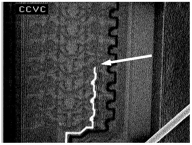
The pieces of equipment necessary to perform CCVC include: a scanning electron microscope, an electrical vacuum feedthrough, a voltage supply, and a switching mechanism to generate dynamic voltages. The scanning electron microscope must scan at or near video rates for adequate CCVC time resolution. Because of the SNR-time resolution tradeoff, a frame-grabbing digital image acquisition system is useful to obtain good signal resolution via averaging. Figure 2 displays a averaged, 16 frame CCVC image of an open conductor in an SRAM. The open (a bit line) site is located at the abrupt change in bright contrast.
CCVC can be used to localize open conductors ( Figure 2 ) and open contacts, but its greatest utility is the identification and verification of conductor logic states on ICs. Note that even though CCVC cannot probe through overlying metal conductors, the continuity of some signal paths can still be verified or inferred by observing regions where the conductor is not covered.
Because capacitive-coupled voltage contrast (CCVC) is relatively easy to set up and perform, it is typically done just before waveform-based voltage contrast. Since CCVC is performed at lower accelerating voltages (typically below 2kV), it can be performed immediately after optical techniques (e.g. light emission, liquid crystal) are performed. It usually makes sense to perform CIVA before CCVC as CIVA is even easier to set up and implement.