System Maintenance occurs every Friday.
System Maintenance occurs every Friday.
Backscatter Electron (BSE) Imaging is a scanning electron microscopy technique that detects differences in atomic number on and below the surface of the sample. In failure analysis, BSE imaging is primarily used to detect sharp atomic number gradients, such as impurities and metal conductor voiding, under IC passivation layers.
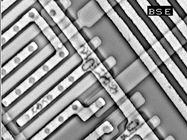
Backscattered electron imaging can locate regions of differing atomic number, such as metal voiding (see Figure 1) and high atomic number impurities, but it normally cannot diagnose the root cause of failure. Numerous mechanisms can cause metal voiding, and high atomic number impurities must be identified by other techniques before their source can be located. Backscattered electron imaging can be an important tool in assisting root cause analysis, but it is rarely used alone.
One should also keep in mind that the primary electron beam energy can be varied to examine the z distribution of backscattered electron anomalies.
Backscatter Electron (BSE) imaging should be performed to examine for metal voiding or high atomic number impurities. The BSE signal is proportional to the atomic number of the sample volume examined; therefore, BSE examination should not be used to identify impurities that have an atomic number similar to the pure sample. Metal voiding in Al conductors produces good BSE image contrast because of the large atomic number difference (0 for the void versus 13 for Al). If a high Z barrier metal, such as TiW, is below the conductor under examination, metal voiding can be difficult to examine using BSE imaging. The large BSE signal from the high Z material can mask and BSE contrast differences caused by the metal void. BSE imaging can still be used to examine metal conductors with barrier metals, but the primary electron beam energy must be controlled so that the BSE signal originates primarily from the top level Al metal and as little BSE signal as possible originates from the barrier metal level.
Backscatter electron imaging requires a scanning electron microscope and a backscattered electron detector. The detector is normally a large area semiconductor positioned directly over the sample. The secondary electron detector can also be used to detect backscattered electrons if the normally positively biased Faraday cage in front of the secondary electron detector's photomultiplier is grounded. This enables the backscatter electrons scattered in the direction of the secondary electron detector to be collected and differentiated from secondary electrons. Since the number of backscattered electrons is far less than the number of secondary electrons generated under the same primary electron beam conditions, beam currents 5 to 10 times greater than those used for secondary electron imaging are normally needed for adequate signal-to-noise ratios.
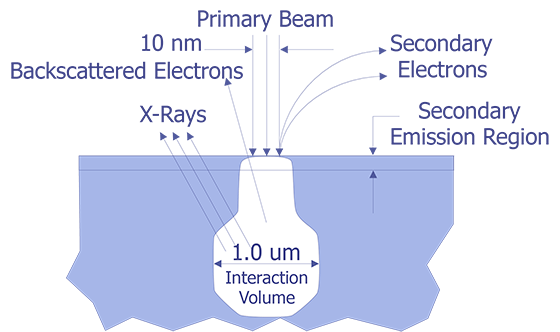
Backscattered electrons are electrons with energies E such that 50 eV < E < E*, where E* is the primary beam energy. Unlike secondary electrons, the backscattered electrons escape from much deeper in the surface, most originating from about 1/3 or less the maximum depth of the electron beam/device interaction volume.

This greatly reduces the surface effects that hamper secondary electron imaging. The major factor determining backscatter electron image contrast is the atomic number of the sample material within the interaction volume, indicating that nuclear scattering is the principle electron interaction. Because of the complex elastic and inelastic scattering processes that create backscatter electrons, no exact theory is possible, but some general comments about image expectations can be made. First, the spatial resolution is limited by the size of the interaction volume at the backscattered electron source; therefore, the spatial resolution will always be less than or equal to the secondary electron image resolution. Second, experimentation with different primary electron beam energies can improve spatial resolution depending upon the backscattered electron source and its depth below the sample surface. Finally, backscattered electron imaging is used primarily to identify metal conductor voiding and verify subsurface composition, and by definition is not a high resolution technique.
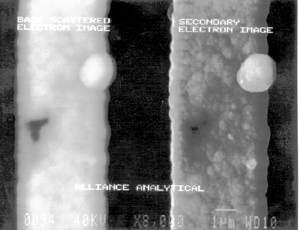
Figure 1 and Figure 3 (see Photographs section) are examples of backscattered electron imaging results. Figure 1 shows metal voiding in a power bus caused by electromigration. The passivation was intact for this image. Figure 3 shows the bright contrast signal that comes from a TiW buried diffusion barrier layer under metal-1 in this two level metal IC. The metal-2 does not have a barrier layer and displays darker image contrast than the metal-1 conductors, even though more of the interaction volume intersects the metal-2 level.
For ICs, backscattered electron imaging should be performed after more benign failure analysis techniques have been applied. The high primary electron beam energies required to generate backscattered electrons from below the IC surface will almost immediately alter the threshold voltage of exposed MOS transistors. This threshold shift results from fixed oxide change and interface trap occupancy in the oxide after exposure to primary electrons and x-rays. If MOS structures are not exposed directly to the high energy primary electron beam, the damage is minimized. Backscattered electron imaging does have the advantage of being able to probe through passivation and, to some extent, metal layers. If backscattered electron examination is indicated by other test methods, it should be applied before layer removal.
For IC test structures such as electromigration serpentines, backscattered electron imaging can be applied after an open conductor or large increase in resistance is indicated. Without a MOS structure to be altered by primary beam irradiation, high energies can be used to ensure that the interaction volume reaches the structures of interest. While surface layer removal can make it easier to reach a buried conductor pattern at lower primary electron beam energies, the possibility of altering the failing conductor state during deprocessing remains a reality. Backscattered electron imaging can eliminate or reduce the need for surface layer removal during failure site localization.