System Maintenance occurs every Friday.
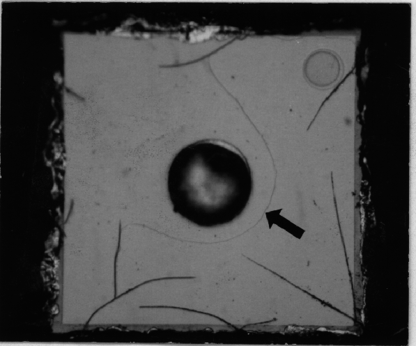
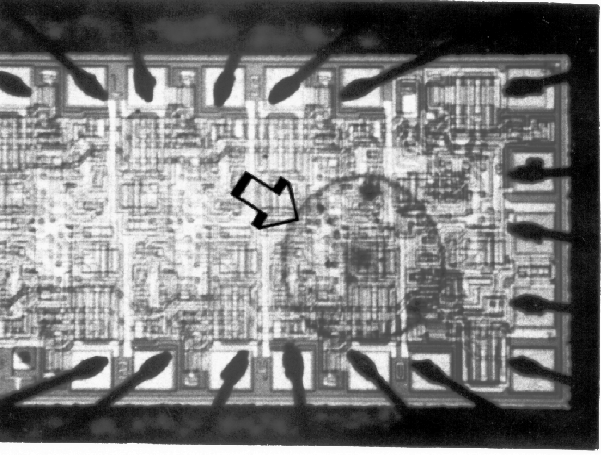
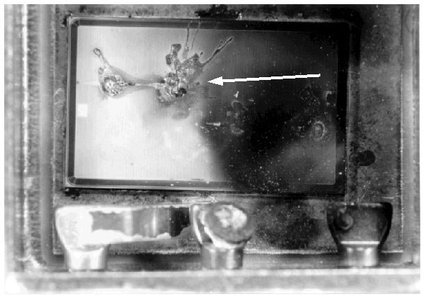
Optical Examination is arguably the most versatile and powerful technique available to the failure analyst. Low power examination is generally regarded as optical examination using a magnification range up to 50X. Optical microscopes that use reflected light are the most common pieces of equipment used to perform a high power examination. A number of failure modes in ICs can be detected by examining the IC at high magnifications using an optical microscope.
An optical microscope system consists of three main components: the magnification system, the light source, and the sample stage. The magnification system can be sub-divided into the objective lenses, the field lens, and the eyepiece.
The objective lenses are one of three types of lenses: achromatic, apochromatic, or non-achromatic. Achromatic lenses are corrected for two colors, normally red and green. Apochromatic lenses are corrected for three colors, normally red, green and violet. Non-achromatic lenses are not corrected for any colors; this means they yield color halos in the formed image. In addition, lenses have a specific magnifying power, numerical aperture rating, and focal length.
The field lens is the lens installed in the column of the microscope between the objective and the eyepiece. Some microscopes come with adjustable field lenses, which allow several differing magnifications to be placed in front of the objective.
The eyepiece can be either a negative (Huggenian), positive (Ramsden), or true negative (Amplifying) lens. Several types of light sources are available for use with optical microscopes. These include low voltage tungsten filament lamps, xenon, mercury vapor lamps, and cesium-iodide lamps. Each has a slightly different color temperature, yielding different color balances. Most stages for failure analysis purposes are regular (non-inverted) stages.
The accurate diagnosis and precise location of failure mechanisms and defects in CMOS ICs are often difficult tasks. Many techniques are available, but successful failure analysis requires careful selection of these techniques and the sequencing of their use. Nondestructive techniques are usually preferred if they are easy to implement and have a high probability of success. Optical microscopy has several desirable attributes, including high spatial sensitivity, simple sample preparation, and absence of special environmental requirements.
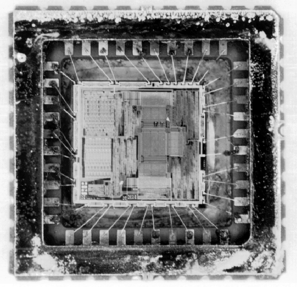
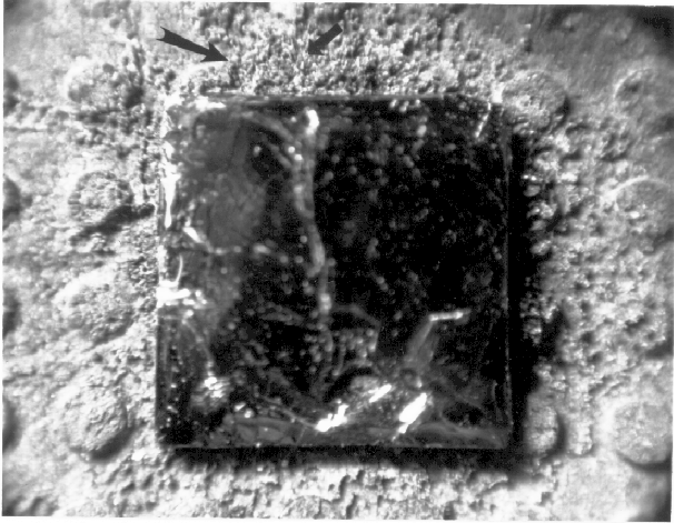
The device to be examined is placed under the optical microscope with the proper lighting, and the surface of the device is examined. Low-power examination can be performed on any suitable sample preparation microscope. These microscopes are available from a number of vendors with numerous configurations and options. The Polaroid MP4 Land Camera system or equivalent provides the best lighting conditions for photographing at low magnifications (below 20X). Above 20X, good quality photographs can be taken on a metallurgical microscope with a low magnification lens. Be sure to avoid hitting the die with the microscope objective, as this can damage both the IC and the objective.
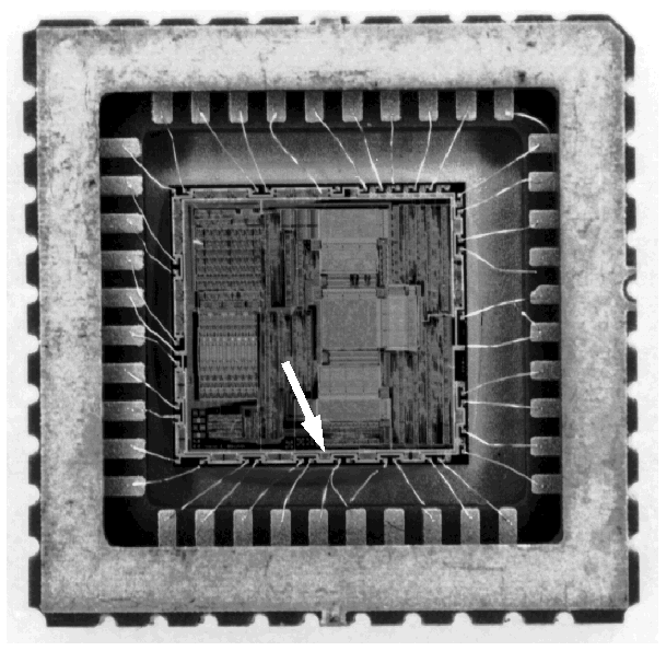
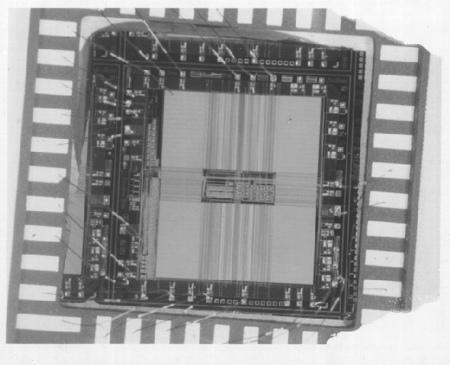
Low-Power Examination is used for CMOS ICs immediately after delidding the IC due to its benign effect on the device and potential for uncovering useful information.
