Are you looking for more information regarding this and other subjects? Look no further than Semitracks' Online Training. Semitracks' Online Training contains short courses and other material useful for any Engineer trying to learn new subjects or brush up on old ones.
What is an External Visual Inspection?
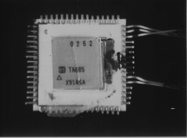
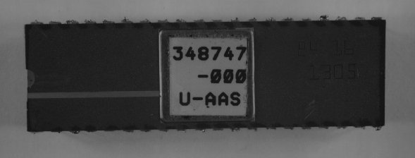
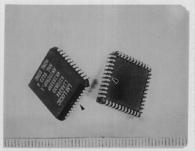
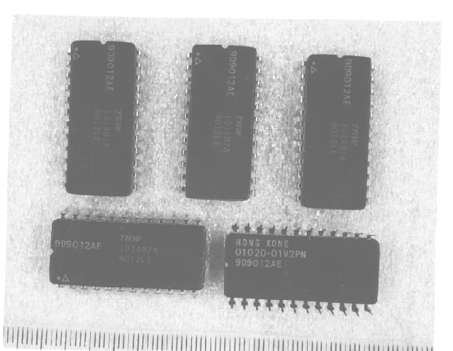
An external visual examination is an examination of the component under a low power optical microscope (1X - 30X). Several aspects of the package are examined: the markings, the condition of the package, and any anomalies associated with the package.
Why Perform an External Visual Examination?
An external visual examination can provide numerous clues pointing to a possible failure mechanism without damaging the circuit further. Failure to perform an external visual examination may result in loss of data on the lid seal, non-permanent markings on the component, and contamination or corrosion.
How is an External Visual Examination Performed?
Normally, an external visual exam is performed with both the naked eye and a low power optical microscope (1X - 30X). The component should be examined on all sides for anomalies, condition, and markings. You should note all of your findings as well as all of the markings you see. When performing an external visual, it is also important to use ESD protection techniques, including placing the component in conductive foam or in a static protection bag when not being examined, using an ESD wrist strap at all times when handling the component outside of the bag, and using a static free work area to examine the component.
When is an External Visual Examination Performed?
Because an external visual examination is non-destructive (even less so than x-ray, electrical testing, or leak testing), this technique should be performed immediately after gathering your historical information and, if possible, before electrical testing.
MIL STD Procedures for External Visual
MIL-STD-883C
METHOD 2009.4
EXTERNAL VISUAL
- PURPOSE. The purpose of this examination is to verify that the materials, design, construction, markings, and workmanship of the device are in accordance with the applicable procurement document. This test would normally be employed at the outgoing inspection from the device manufacturer's facility or as an incoming user inspection. This test may also be utilized to inspect for damage due to handling and mounting of the devices.
- APPARATUS. Apparatus used in this test shall be capable of demonstrating device conformance to the applicable requirements, which may include optical equipment capable of magnification between 1.5X and 3X and a relatively large and accessible field of view such as an illuminated ring magnifier.
- PROCEDURE. The device shall be examined under a magnification of 1.5 X minimum (unless otherwise specified) with a field of view sufficiently large to contain the entire device in accordance with the requirements of the applicable procurement specification and the criteria listed in 3.1. Where adherence of foreign material is in question, devices may be subjected to a clean filtered air stream (suction or expulsion) of 88 feet per second maximum, and re-inspected.
- Failure criteria. Devices shall be considered to fail if they exhibit any of the following:
- Device design, lead (terminal) identification, markings (content, placement, and legibility), materials, construction, and workmanship are not in accordance with the applicable specification or drawing.
- Ceramic packages with brazed leads or leads exiting through the sealing glass which exhibit any of the following:
- Cracked or broken packages except where the crack would lead to chip-out acceptable below. Surface scratches shall not in themselves be cause for rejection.
- Any chip-out that exposes either sealing glass (not previously exposed prior to the chip out) or any lead frame material that is not intended to be exposed by design. See Figure 2009-1.
- Any chip-out dimension that exceeds 0.060 inches in any direction on the surface and has a depth which exceeds 25 percent of the thickness of the affected package element (e.g., cover, base or wall).
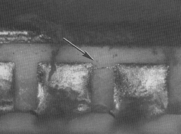
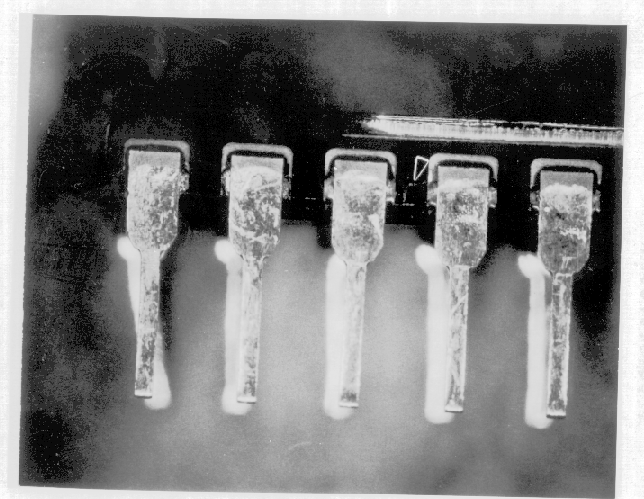
- Visible evidence of corrosion, contamination or breakage, grossly bent or broken leads, cracked seals or defective (peeling, flaking, or blistering) plating or evidence of plating non-adhesion. (Discoloration of the finish shall not be cause for failure unless there is evidence of flaking, pitting, or corrosion.)
- External lead metallization forming a conductor to a brazed pin which exhibits voids greater than 25 percent of its width.
- Leads with pits and/or depressions which exceed 25 percent of the width (diameter for round leads) and are greater than 0.005 inch in depth.
- Leads with burrs exceeding a height of 0.005 inch.
- Lead misalignment to the braze pad to the extent that less than 75 percent of the lead braze section is brazed to the pad.
- Bridged metallization in which the isolation between leads or between lead and other package metallization is reduced to less than 50 percent of the design minimum.
- Braze material flow, or other foreign material (i.e., contamination or corrosion) which reduces the isolation between leads or between braze pads to less than 50 percent of design minimum.
- Protrusions on the bottom (mounting) surface of the package which extend beyond the seating plane.
- Protrusions (excluding glass run out) on any other package surface which exceeds 0.015 inch in height.
- Evidence of delamination on any multilayer ceramic package.
- Braze material which increases the lead dimensions to greater than 0.005 inch above the design maximum between the seating plane and the ceramic body or which increases the lead dimensions to greater than the design maximum below the seating plane.
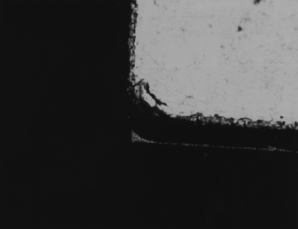
- Any evidence of cracking or crazing in glass which forms the final package seal.
- Metal or ceramic packages with hard glass-to-metal seals which exhibit any of the following:
- Visible evidence of corrosion, contamination or breakage, grossly bent or broken leads, cracked seals (except for glass meniscus), defective (peeling, flaking, or blistering) plating or evidence of plating non-adhesion. (Discoloration of the finish shall not be cause for failure unless there is evidence of flaking, pitting, or corrosion.)
- Leads which are not intact and aligned in their normal location, free of sharp or unspecified lead bends, and (for ribbon leads) free of twist outside the normal lead plane.
- Leads which are not free of foreign material such as paint or other adherent deposits, or dust.
- Foreign material which bridges between pins or between a pin and a conductive package element.
- Leads with pits and/or depressions which exceed 25 percent of the width (diameter for round leads) and are greater than 0.005 inch in depth.
- Leads with burrs exceeding a height of 0.005 inch.
- Defects in the sealing glass between package elements which exhibit any of the following:
- Crazing of glass-seal surface (See Figure 2009-2).
- Radial cracks that originate at the case body glass-to-metal and propagate inward toward the leads. (See Figure 2009-3).
- Radial or circumferential cracks which extend beyond, or are located in, the region beyond the midpoint of distance from the lead to the case. (See Figure 2009-4 and Figure 2009-5).
- Any single circumferential crack (or overlapping cracks) which do(es) not lie completely within a single quadrant (i.e., extends beyond 90 arc or rotation about the lead) (See Figure 2009-5).
- Meniscus cracks, except those located within 1/2 the distance between the lead and the case (metal-to-metal). (See Figure 2009-6.) The glass meniscus is defined as that area of glass which wicks up the lead or terminal. Hair-line cracks occurring in the glass meniscus are called meniscus cracks (See Figure 2009-7).
- Reentrant seals which exhibit non-uniform wicking (i.e., negative meniscus) at the lead and/or body interface. (See Figure 2009-8.)
- Ceramic packages without leads (e.g., leadless chip carriers) which exhibit any of the following:
- Surface contamination with loose foreign or intrinsic material (ceramic gold, etc.), visible evidence of corrosion and stains or discoloration, exclusive of variations of gold plating color.
- Ceramic cracks, voids and holes.
- Ceramic chip-outs, and open or closed bubbles that dimensionally exceed .030 inch in any direction on the affected surface (edge or corner), and exceed a depth of 25 percent of the thickness of the affected package element (e.g., cover, lid, base or wall).
- Delamination of any plated or laminated structure.
- Any evidence of cracking or crazing in the sealing glass between the cover (lid) and body.
- Lid or cover protrusions that exceed .005 inch in height.
- Protrusions that exceed .005 inch in height beyond the surface plane of the solder pads.
- Bridged metallization (not intended by design) between solder pads, between elements of thermal patterns and between seal ring or lid to metallized castellations.
- Metallization peeling, flaking or blistering.
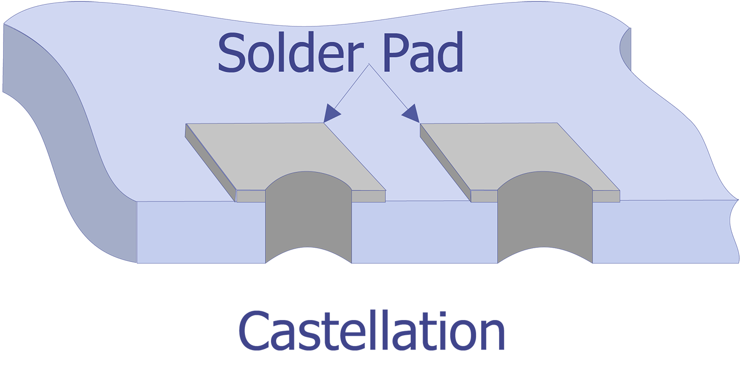
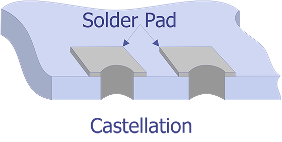
- Castellation to solder pad misalignment. (The castellation shall lie within the boundaries of the solder pad). (See Figure 2009-9.)
- Castellation depth, width and package edge misalignment. (The castellation depth and width, clear opening along its length, shall not be less than .004" and .009", respectively, regardless of reasons, including misalignment due to ceramic layer shifting and taper.) (See Figure 2009-10.)
- Evidence of any nonconformance with the detail drawing or applicable procurement document, absence of any required feature, or evidence of damage, corrosion, or contamination which will interfere with the normal application of the device.
- Any visible scratch, mar, or indentation in the surface finish of the lead above the seating plane that extends more than l/2 the width of the lead and severely damages the finish or exposes base metal.
- SUMMARY. The following details shall be specified in the applicable procurement document:
- Requirements for markings and the lead (terminal), or pin identification.
- Detailed requirements for materials, design, construction, and workmanship.
- Magnification if other than specified.
References on External Visual Inspection
- Ed Doyle Jr. and Bill Morris, Microelectronic Failure Analysis Techniques A Procedural Guide, IIT Research Institute, 1980, Section III-L.
- John Devaney, Gerald Hill, and Robert Seippel, Failure Analysis, Failure Recognition and Training Services, 1983, pp. 4.2-4.5