Are you looking for more information regarding this and other subjects? Look no further than Semitracks' Online Training. Semitracks' Online Training contains short courses and other material useful for any Engineer trying to learn new subjects or brush up on old ones.
What is a Curve Trace?
A curve trace is produced by an electrical test that usually measures the current (I) that results from applying a voltage (V) varied over a range from one voltage value to another value. This particular module deals specifically with curve trace measurements made on the I/O pins for continuity or for other parametric issues, such as input leakage, output drive currents, output voltage levels, etc.
A curve trace measurement is made using a curve tracer, parameter analyzer, or other electrical test equipment. This type of test is typically performed at a bench setup to complement automatic test equipment (ATE) data or replace it when ATE testing is not feasible. The display or plot of current versus voltage obtained from this test is referred to as a curve trace or I-V measurement. Curve traces can also be V-V or V-I measurements or even V vs. time or I versus time if necessary.
Curve trace measurements can provide insight into numerous failure mechanisms that can affect the I/O pins, including EOS, ESD, bond wire problems, and packaging problems. Another advantage of curve tracing is its ease of setting up, low cost, non-destructive nature, and flexibility.
How is a Curve Trace Performed?
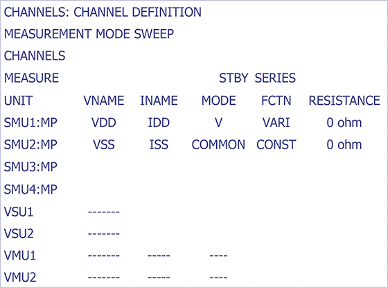
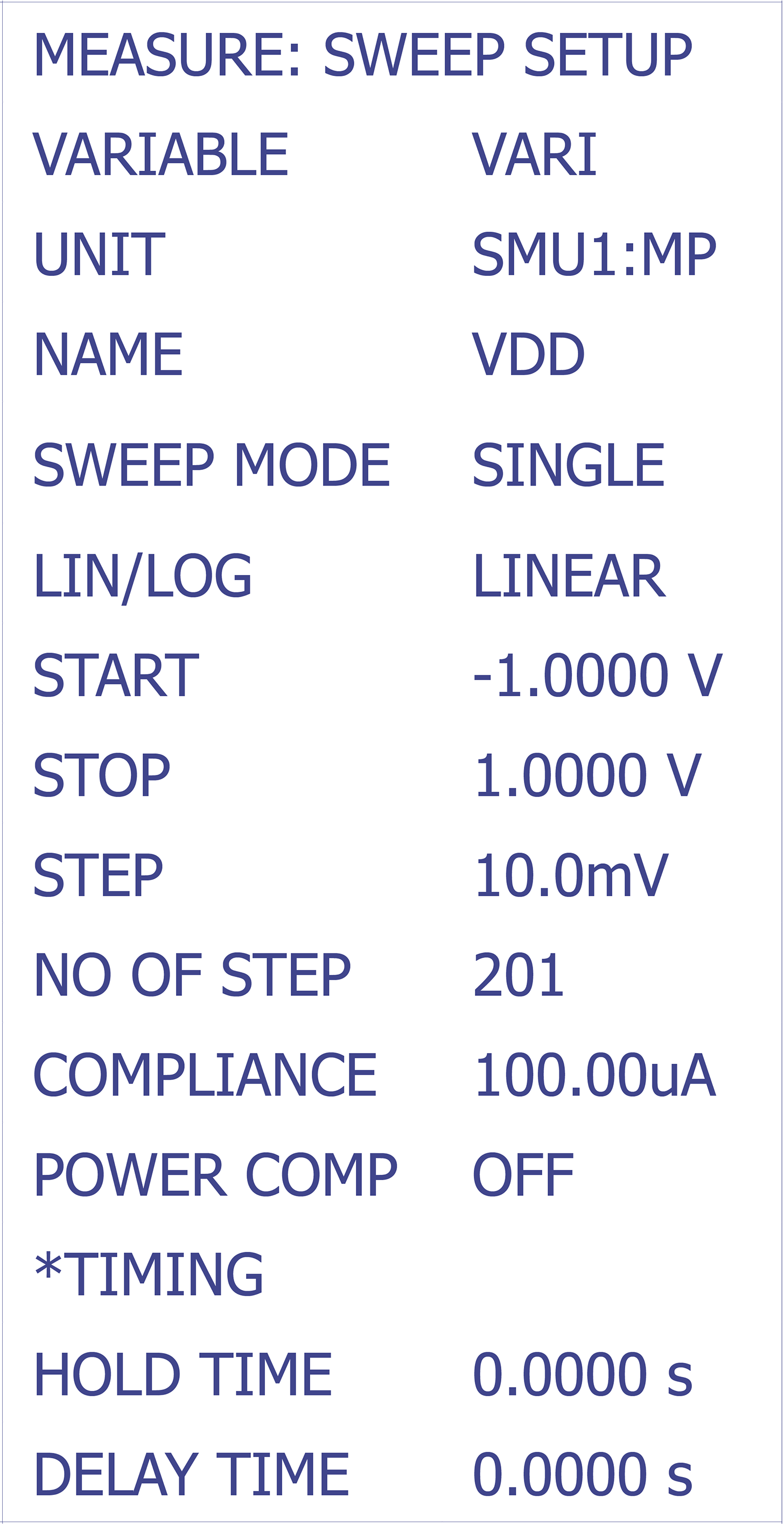
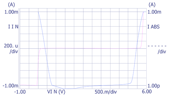
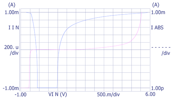
The typical curve trace test method is to force a voltage and measure the resultant current one pin at a time to evaluate continuity or leakage current. Curve trace I-V measurements are made with instruments such as the Tektronix 576 or HP4145 Semiconductor Parameter Analyzer. The Tektronix 576 is an analog instrument commonly used to provide a real time display of the current and voltage while the voltage continuously sweeps from a negative voltage through zero to a positive voltage and back to the negative voltage (AC mode). The HP4145 is a digital instrument that can display the current and voltage with the voltage incrementally stepped between two values. The HP4145 can provide both linear and logarithmic displays, save data in internal files and on floppy diskettes, and send data to other equipment, such as a plotter. An example of an HP4145 curve trace for an input pin (outer trace) and output pin (inner trace) of a CMOS IC is shown below. For this measurement, one of the HP4145 channels was used to increment the input pin voltage from -1 V to 1 V with VDD and another channel was used to hold VDD and VSS at 0 V.
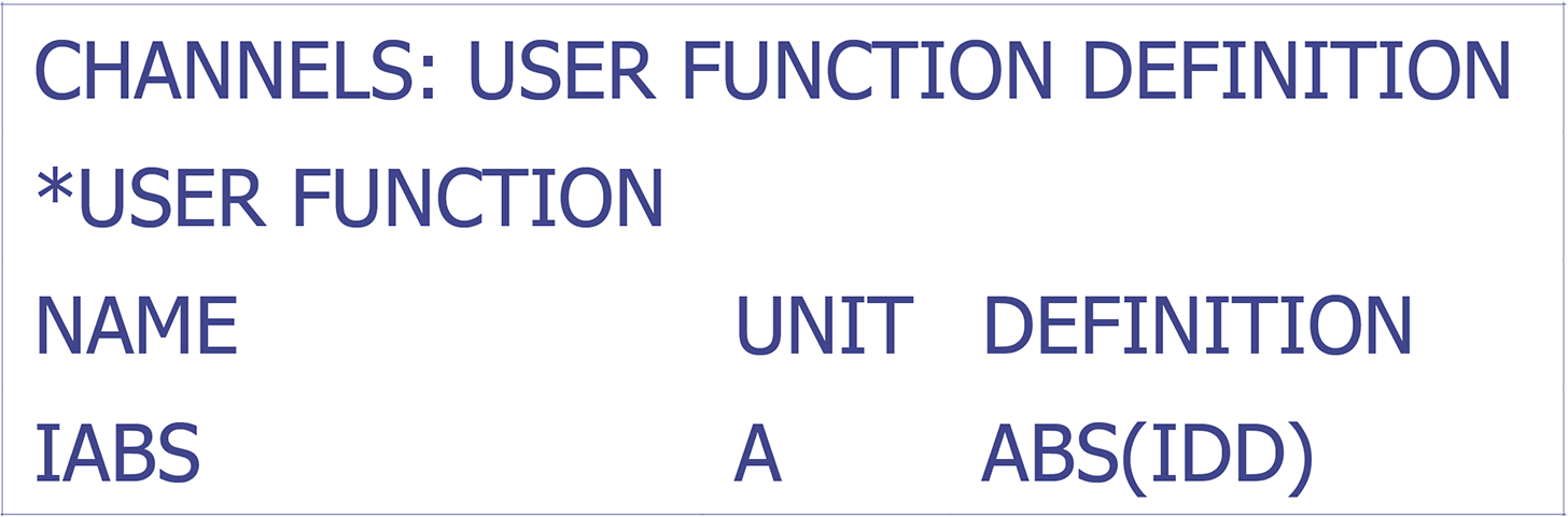
When you examine an input, output, or bi-directional pin using a curve tracer or a parameter analyzer, several distinct curves can be identified and associated with possible failure mechanisms. If the IC is not passing continuity, the leakage curve you will examine is created when the VDD and VSS pins are connected to ground and a voltage sweep is performed on the pin in question. To perform a logarithmic curve of this sweep on an HP4145 parameter analyzer, enter an appropriate name in the USER FCTN box at the Channel Definition screen. Make the expression an absolute value expression of the current. This will allow you to view the logarithmic plot of the current and examine both positive and negative values of current at the same time. If you are unable to do this with your particular piece of equipment, it will not be a problem-- you will just have to do a little more interpretation in your head.
How to define channels on the HP4155.How to set up the measurement sweep.How to enter a variable to allow absolute value plotting.An example plot of a leakage curve between VDD and VSS.
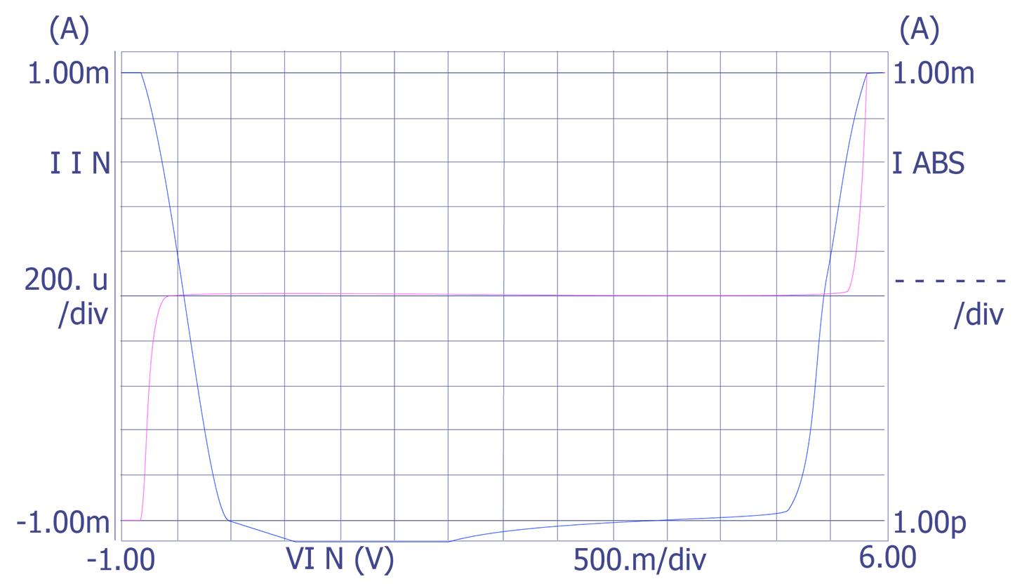
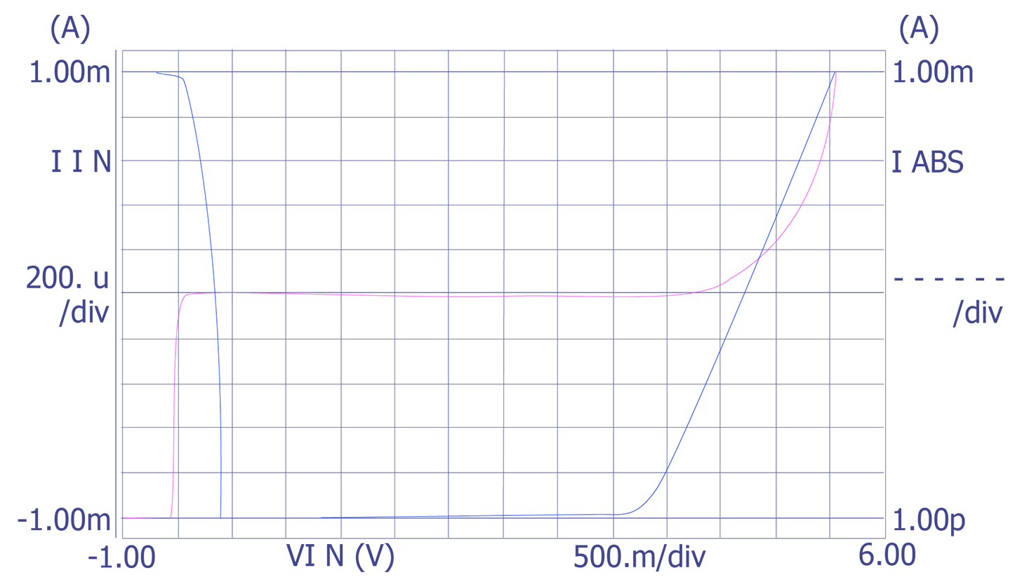
After you have set up the parameter analyzer, take the measurement. To do this, place the component in a static burn-in configuration, except for the pin to be measured. Sweep the voltage on this pin from 1 volt below VSS to 1 volt above VDD. Be sure that the compliance is set to 10 mA or less on the supplies for VDD and VIN. Either the leakage will be normal (at or below the limits set for the IC), or it will be excessive (above the limits set for the IC). Figure 5 is an example plot of normal leakage levels for an input pin.
An example plot of normal leakage levels for an input pin.
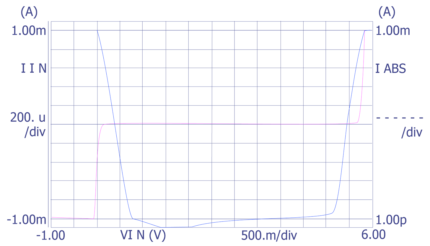
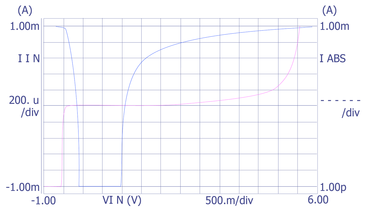
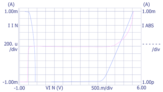
Figure 6 is an example of an input pin with excessive leakage when the pin is in a low state. This is equivalent to excessive low level input leakage (IIL).
An example of an input pin with excessive leakage when the pin is in a low state.
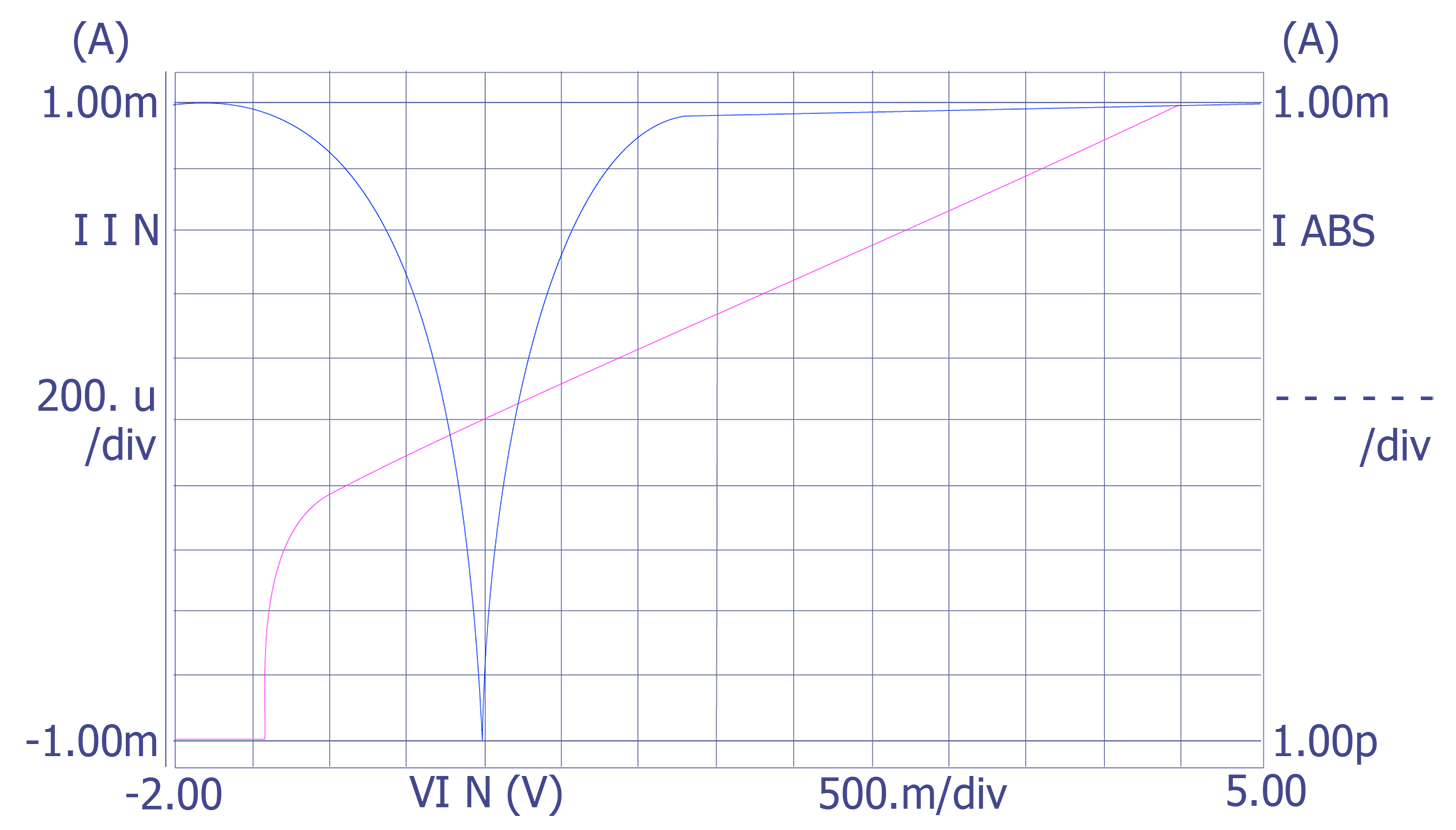
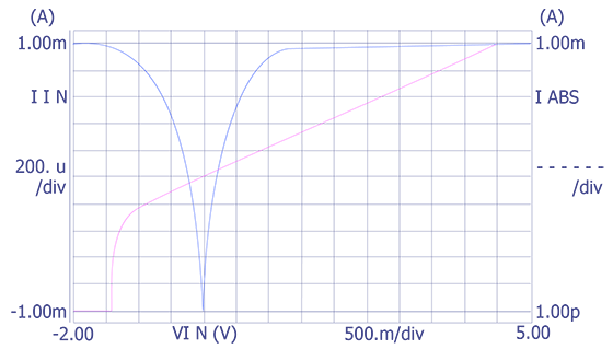
Both logarithmic and linear plots of the pin characteristic can yield useful information. Three types of curves are typically associated with input and output leakage and their associated defects.
A linear leakage curve. This type of leakage tends to occur with electrostatic discharge (ESD) damage or electrical overstress (EOS). Figure 7 is an example of this type of leakage.
A linear leakage curve.
A parabolic leakage curve. This type of leakage usually occurs when a parasitic MOS transistor is biased on. This situation can occur as the result of design errors, or ionic contamination introduced during fabrication or packaging. Figure 8 is an example of this type of leakage.
A parabolic leakage curve.
An exponential leakage curve. This type of leakage usually indicates incorrect junction leakage or abnormal transistor operation (such as second breakdown operation) in I/O buffers. Abnormal junction leakage can be the result of incorrect design, incorrect doping profiles, overalloyed junctions, or electrostatic discharge (ESD). In order to tell if the leakage phenomenon is exponential, it is usually necessary to examine the leakage using a logarithmic plot in conjunction with a linear plot. Exponential current leakage will show up as a straight line on a logarithmic plot. Figure 9 is an example of this type of leakage.
An exponential leakage curve.
In a few instances, the leakage curve may not be linear, parabolic or exponential. If the curve is sub-linear, respond with linear as a answer. Some gate oxide shorts or electrostatic discharge (ESD) damage may be sub-linear. If the curve is sub-exponential, but definitely not parabolic, answer exponential. Again, some gate oxide shorts and electrostatic discharge (ESD) damage may be sub-exponential.
Continuity testing on a CMOS IC
To perform continuity testing on a CMOS IC, obtain a switchbox or similar electrical fixture to allow independent control of the IC pins. The most useful type of switchbox is one where the pins can be set to a high rail, low rail, or controlled independently. Once the fixturing is set up, tie all of the pins to ground or the low rail. Set a current limit of 10 uA so that no damage will occur. Connect pin 1 to the other terminal of the curve tracer or parameter analyzer. Sweep the voltage on pin 1 from -1 volts to +1 volts. Repeat this test for all of the pins on the IC. For I/O pins, the curve should exhibit forward diode characteristics in both directions. For the VDD pin(s), the curve should have a forward diode characteristic in the negative direction only. For the VSS pin(s), the curve should have a forward diode characteristic in the positive direction only.
The following conditions are possible: open in both directions, short or resistive characteristic, open in one direction. Explain what failure mechanisms may cause the conditions.
Continuity testing on a bipolar IC
To perform continuity testing on a bipolar IC, obtain a switchbox or similar electrical feature. Once the fixturing is set up, you can measure electrical continuity between each of the I/O pins and the power supply pins (VCC and GND). Be sure to set the current limit to 10 uA or less to avoid damaging any junctions. To do this for continuity to VDD, sweep the voltage from -1 volt to the maximum supply voltage. For VSS, sweep the voltage from -1 volt to the maximum supply voltage. The curves should exhibit a diode in one direction and negligible leakage (1 nA or less) in the other direction.
Input leakage testing
To perform input leakage testing, you must place the IC in a powered up condition. The static burn-in configuration works well for this measurement. Connect one terminal to VCC, attach the second terminal to GND, and set the third terminal to perform a voltage sweep from -1 volt to VCC + 1 volt. This curve will yield information on both high level input leakage and low level input leakage. The shape of the curve can also yield information on the nature of the defect.
Output drive current testing
Depending on the nature of the failure and complexity of the IC, output drive current testing may or may not be possible. To obtain this curve, first set up the IC in a condition where the suspect output pin will be in a logical "1" state. Sweep the voltage from VCC to VCC/2 while monitoring the current. The curve will yield information on the output drive current. Normally, output drive current is specified for some voltage level below VCC. The current value can be obtained from the curve. Repeat the test with the IC set up in a condition where the suspect output pin wll be in a logical "0" state. Sweep the voltage from 0 to VCC/2 while monitoring the current. The curve will yield information on the low level output drive current.
Output voltage level testing
Output voltage level testing, like output drive current, may or may not be possible depending on the nature of the failure and the complexity of the IC. To obtain this data, first set up the IC in a condition where the suspect output pin will be in a logical "1" state. Sweep the current from 0 to the maximum rated drive current while monitoring the voltage level on the output pin. At the maximum rated drive current, the output drive voltage should be within some specified voltage of VCC. Repeat the test with the suspect output pin in the logical "0" state, sweeping the current from 0 to the maximum rated sink current. At the maximum current, the output drive voltage should be within some specified voltage on GND.
Tri-state leakage
Tri-state leakage testing, like output drive current, may or may not be possible depending on the nature of the failure and the complexity of the IC. To obtain this data, first set up the IC in a condition where the suspect I/O pin will be tri-stated or in a high impedance mode. Sweep the voltage from 0 to VCC while monitoring the current level on the I/O pin. At VCC and GND, the leakage current should be within some specified value (usually 10's of nA or less).
Why is a Curve Trace Performed?
A curve trace is commonly used for continuity or leakage current measurements. This electrical test method is also used to obtain I-V curves for diodes and a family of operating curves for devices such as bipolar or MOS transistors. Another common usage is for IDDQ vs. VDD measurements for CMOS ICs. This type of measurement is preferred over a measurement of current at a single voltage for several reasons:
(1) the curve trace instrument can provide more precise control over the maximum current, voltage, or power to ensure that the failure mechanism is not altered and that the component is not damaged, and
(2) the I-V curve can provide useful information about the stability and nature of the failure mechanism.
When is a Curve Trace Performed?
A curve trace is usually performed as one of the initial electrical measurements during analysis of a component. It would typically be used first to assure that proper electrical continuity exists to all of the pins or other connections of the component. It would be used to attempt to confirm the failure symptoms. For example, a curve trace could be used to confirm an input pin leakage failure.
MIL STD Procedures for High Level Output Voltage
MIL-STD-883C
METHOD 3006.1
HIGH LEVEL OUTPUT VOLTAGE
PURPOSE. This method establishes the means for assuring circuit performance to the limits specified in the applicable procurement document in regard to HIGH level output drive, which may be specified as a minimum value VOH min. or as a maximum VOH max. This method applies to digital microelectronic devices, such as TTL, DTL, RTL, ECL and MOS.
APPARATUS. The test instrument shall be capable of loading the output of the circuit under test with the specified positive or negative currents (IOH). Resistors may be used to simulate the applicable current levels. The test instrument shall also be capable of supplying the worst case power supply and input voltages. The test chamber shall be capable of maintaining the device under test at any specified test temperature.
PROCEDURE. The device shall be stabilized at the specified test temperature. Worst case power supply voltages and worst case input levels including guaranteed noise margins shall be applied to the test circuit to provide a HIGH level output. Forcing current, equal to the circuit worst case high level fan out, shall then be applied to the test circuit output terminal and the resultant output voltage measured. The output measurement shall be made after each input is conditioned.
SUMMARY. The following details shall be specified in the applicable procurement document:
Test temperature.
Current to be forced from or into output terminal.
Power supply voltage(s).
Input levels.
VOH min. or VOH max. limits.
MIL STD Procedures for Low Level Output Voltage
MIL-STD-883C
METHOD 3007.1
LOW LEVEL OUTPUT VOLTAGE
PURPOSE. This method establishes the means for assuring circuit performance to the limits specified in the applicable procurement document with regard to LOW level output drive which is specified as a maximum value (VOL max) or a minimum value (VOL min). This method applies to digital microelectronic devices, such as TTL, DTL, RTL, ECL and MOS.
APPARATUS. The test instrument shall be capable of loading the output of the circuit under test with the specified positive or negative currents (IOL). Resistors may be used to simulate the applicable current levels. The test instrument shall be capable of supplying the worst case power supply and input voltages. The test chamber shall be capable of maintaining the device under test at any specified temperature.
PROCEDURE. The device shall be stabilized at the specified test temperature. Worst case power supply voltages and worst case input levels including guaranteed noise margins shall be applied to the test circuit to provided LOW level output. Forcing current, equal to the circuit worst case LOW level fan outs shall be applied to the test circuit output and the resultant output voltage measured. The output measurement shall be made after each input is conditioned.
SUMMARY. The following details shall be specified in the applicable procurement document:
Test temperature.
Current to be forced into or from the output terminal.
Power supply voltage(s).
Input levels.
VOL max or VOL min limits.
MIL STD Procedures for Input or Output Breakdown Voltage
MIL-STD-883C
METHOD 3008.1
BREAKDOWN VOLTAGE, INPUT OR OUTPUT
PURPOSE. This method establishes the means for assuring device performance to the limits specified in the applicable procurement document in regard to input and output breakdown voltage symbolized as VIH (max), VOH (max), VIL (min), and VOL (min) as applicable. This method applies to digital microelectronic devices, such as TTL, DTL, RTL, ECL and MOS.
APPARATUS. The test chamber shall be capable of maintaining the device under test at any specified temperature.
Method A. This test is generally performed to assure that breakdown does not occur on a device. An instrument shall be provided that has the capability of forcing a specified voltage at the input or output terminal of the test circuit and measuring the resultant current flowing in that terminal. The test instrument shall also have the capability of applying voltage levels to all other terminals. Care should be taken to assure that the test equipment does not inadvertently apply voltage to the device under test that will exceed the maximum rating of each terminal and that the current from the test equipment is sufficiently limited so that the device is not destroyed. This method can also be used to test the ability of power supply terminals to withstand a voltage overload.
Method B. This test is generally performed to assure that breakdown does occur on a device as specified in the applicable procurement document. An instrument shall be provided that has the capability of forcing a specified current at the input or output terminal of the test circuit and measuring the resultant voltage at that terminal. The test instrument shall also have the capability of applying voltage levels to all other terminals. Care should be taken to assure that the test equipment does not inadvertently apply voltage to the device under test that will exceed the maximum rating of each terminal so that the device is not destroyed. The minimum compliance voltage of the current source shall be specified when applicable.
PROCEDURE. The device shall be stabilized at the specified test temperature.
Method A. All terminals, with the exception of the test terminal, shall be conditioned according to the applicable procurement document. A prescribed voltage shall be applied to the designated input or output terminal and the resultant current measured. then testing for breakdown, all input and output terminals shall be tested individually. At the conclusion of the test, the device shall be functional.
Method B. All terminals, with the exception of the test terminal, shall be conditioned according to the applicable procurement document. The specified current shall be forced at the designated input or output terminal, and the voltage at the terminal measured. At the conclusion of the test, the device shall be functional.
SUMMARY. The following details shall be specified in the applicable procurement document:
Test temperature.
Forced voltages (Method A).
Conditioning voltages for all other terminals.
Forced current (Method B).
Maximum breakdown current limits (Method A).
Minimum breakdown terminal voltage (Method B).
MIL STD Procedures for Low Level Input Current
MIL-STD-883C
METHOD 3009.1
INPUT CURRENT, LOW LEVEL
PURPOSE. This method establishes the means for assuring circuit performance to the limits specified in the applicable procurement document in regard to LOW level input load which may be specified as a minimum value (IIL min) or as a maximum value (IIL max)). This method applied to digital microelectronic devices, such as TTL, DTL, RTL, ECL and MOS.
APPARATUS. The test chamber shall be capable of maintaining the device under test at any specified test temperature. An instrument shall be provided that has the capability of applying the worst case LOW voltage to the input terminal of the test circuit, (and worst case levels on the other inputs), and measuring the resultant current at the input terminal.
PROCEDURE. The device shall be stabilized at the specified test temperature. Worst case power supply voltages and worst case input voltages shall be applied to the test circuit and the resultant current at the input terminal shall be measured. Inputs shall be tested individually.
SUMMARY. The following details shall be specified in the applicable procurement document:
Test temperature.
Power supply voltages.
Input voltage.
Voltages at other input terminals which cause worst case current at the input under test.
IIL max or IIL min.
MIL STD Procedures for High Level Input Current
MIL-STD-883C
METHOD 3010.1
INPUT CURRENT, HIGH LEVEL
PURPOSE. This method establishes the means for assuring circuit performance to the limits specified in the applicable procurement document in regard to HIGH level input load which may be specified as a maximum value (IIH max) or a minimum value (IIH min). This method applies to digital microelectronic devices, such as TTL, DTL, RTL, ECL and MOS.
APPARATUS. The test chamber shall be capable of maintaining the device under test at any specified temperature. An instrument shall be provided that has the capability of applying the worst case HIGH voltage to the input terminal of the test circuit, and worst case levels at the other inputs, and measuring the resultant current at the input terminal.
PROCEDURE. The device shall be stabilized at the specified test temperature. Worst case power supply voltages and worst case input voltages shall be applied to the test circuit and the resultant current at the input terminal shall be measured. Inputs shall be tested individually.
SUMMARY. The following details shall be specified in the applicable procurement document:
Test temperature.
Power supply voltages.
Input voltage.
Input voltages at other input terminals which cause worst case current at the input under text.
IIH max.
MIL STD Procedures for Output Short Circuit Current
MIL-STD-883C
METHOD 3011.1
OUTPUT SHORT CIRCUIT CURRENT
PURPOSE. This method establishes the means for assuring circuit performance to the limits specified in the applicable procurement document in regard to output short circuit current (IOS). This method applied to digital microelectronic devices, such as TTL, DTL, RTL and MOS.
APPARATUS. A test chamber capable of maintaining the device under test at any specified temperature. An instrument will be provided that has the capability of forcing a voltage specified in the applicable procurement document at the output terminal of the device under test and measuring the resultant current flowing in that terminal. The test instrument shall also have the capability of applying specified voltage levels to all other inputs.
PROCEDURE. The device shall be stabilized at the specified test temperature. Each output per package shall be tested individually.
TTL, DTL, RTL, MOS (P-Channel and N-Channel). Inputs of the device under test shall be conditioned in such a way as to provide a HIGH level at the output for TTL, DTL, RTL, and MOS (N-Channel) and a LOW level at the output for MOS (P-Channel). The output terminal shall be forced to 0 volt potential and the resultant current flow measured.
C-MOS IOSH. Inputs of the device under test shall be conditioned in such a way as to provide a HIGH level at the output. The output terminal shall be forced to 0 volt potential and the resultant current flow measured.
C-MOS IOSL. Inputs of the device under test shall be conditioned in such a way as to provide a LOW level at the output. The output terminal shall be forced to a voltage potential specified in the procurement document and the resultant current flow measured.
SUMMARY. The following details shall be specified in the applicable procurement document:
Test temperature.
Input conditioning voltages.
Power supply voltages.
IOS max and IOS min limits.
MIL STD Procedures for Terminal Capacitance
MIL-STD-883C
METHOD 3012.1
TERMINAL CAPACITANCE
PURPOSE. This method establishes the means for assuring circuit performance to the limits specified in the applicable procurement document in regard to terminal capacitance. This method applies to digital microelectronic devices, such as TTL, DTL, RTL, ECL and MOS.
APPARATUS. The instrument shall be capable of applying a 1 MHz controllable amplitude signal superimposed on a variable plus or minus DC voltage. The instrument will also have the capability of measuring the capacitance of this terminal to within the limits and tolerance specified in the applicable procurement document.
PROCEDURE. This test may be performed at 25C +-3C. The capacitance measuring bridge shall be connected between the input or output terminal and the ground terminal of the test circuit. The bridge shall be adjusted for a signal of 1 MHz, riding a bias level specified in the applicable procurement document; the signal amplitude shall not exceed 50 mVRMS. With no device in the test socket the bridge shall then be zeroed. For capacitance values below 20 pF, the device shall be connected directly to the bridge with leads as short as possible to avoid the effects of lead inductance. After inserting the device under test and applying the specified bias conditions, the terminal capacitance shall be measured and compared to the limits listed in the applicable procurement document.
SUMMARY. The following details shall be specified in the applicable procurement document:
Circuit bias conditions.
Bias level at which measurements are to be made.
Maximum capacitance limits.
MIL STD Procedures for Noise Margin Measurements for Digital ICs
MIL-STD-883C
METHOD 3013.1
NOISE MARGIN MEASUREMENTS FOR DIGITAL MICROELECTRONIC DEVICES
PURPOSE. This method establishes the means of measuring the DC (steady state) and AC (transient) noise margin of digital microelectronic devices or to determine compliance with specified noise margin requirements in the applicable procurement document. It is also intended to provide assurance of interchangeability of devices and to eliminate misunderstanding between manufacturers and users on noise margin test procedures and results. The standardization of particular combinations of test parameters (e.g., pulse width, pulse amplitude, etc.,) does not preclude the characterization of devices under test with other variations in these parameters. However, such variations shall, where applicable, be provided as additional conditions of test and shall not serve as a substitute for the requirements established herein.
Definitions. The following definitions shall apply for the purposes of this test method:
Noise margin. Noise margin is defined as the voltage amplitude of extraneous signal which can be algebraically added to the noise-free worst case "input" level before the output voltage deviates from the allowable logic voltage levels. The term "input" (in quotation marks) is used here to refer to logic input terminals or ground reference terminals.
DC noise margin. DC noise margin is defined as the DC voltage amplitude which can be algebraically added to the noise-free worst case "input" level before the output exceeds the allowable logic voltage levels.
AC noise margin. AC noise margin is defined as the transient or pulse voltage amplitude which can be algebraically added to the noise-free worst case "input" level before the output voltage exceeds the allowable logic voltage levels.
Maximum and minimum. Maximum and minimum refer to an algebraic system where "max" represents the most positive value of the range and "min" represents the least positive value of the range.
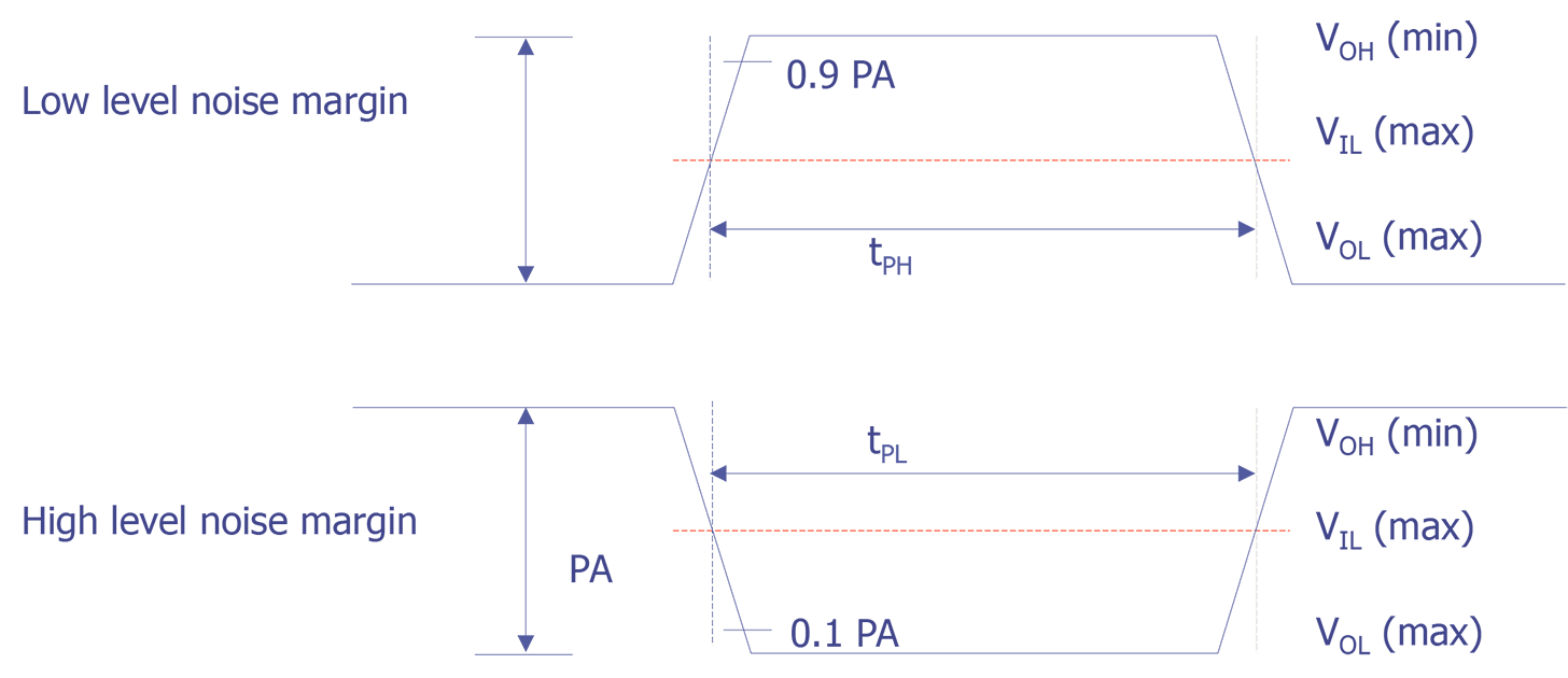
Symbols. The following symbols shall apply for the purposes of this test method and shall be used in accordance with the definitions provided (see 1.2.1, 1.2.2, and 1.2.3) and depicted in Figure 1, Figure 2, and Figure 3
Logic levels.
VIL max: The maximum allowed input LOW level in a logic system.
VIL min: The minimum allowed input LOW level in a logic system.
VIH max: The maximum allowed input HIGH level in a logic system.
VIH min: The minimum allowed input HIGH level in a logic system.
VOL max: The maximum output LOW level specified for a digital microelectronic device.
VOL max is also the noise-free worst case input LOW level
VOL (max) < VIL (max)
VOH min: The minimum output HIGH level specified for a digital microelectronic device.
VOH min is also the noise-free worst case input HIGH level.
VOH (min) > VIH (min)
Noise margin levels
VNL: The LOW level noise margin or input voltage amplitude which can be algebraically added to VOL (max) before the output level exceeds the allowed logic level.
VNH: The HIGH level noise margin or input voltage amplitude which can be algebraically added to VOH (min) before the output level exceeds the allowed logic level.
VNG+: The positive voltage which can be algebraically added to the ground level before the output exceeds the allowed logic level determined by worst case logic input levels.
VNG-: The negative voltage which can be algebraically added to the ground level before the output exceeds the allowed logic level determined by worst case logic input levels.
VNP+: The positive voltage which can be algebraically added to the noise-free worst case most positive power supply voltage before the output exceeds the allowed logic level determined by worst case logic input levels.
VNP-: The negative voltage which can be algebraically added to the noise-free worst case most negative (least positive) power supply voltage before the output exceeds the allowed logic level determined by worst case logic input levels.
10 percent and 90 percent amplitude levels. The pulse repetition rate shall be sufficiently low that the element under test is at steady-state conditions prior to application of the noise pulse. For the purpose of this criteria, doubling the repetition rate or duty cycle shall not affect the outcome of the measurement.
Load. The load for this test shall simulate the circuit parameters of the normal load which would be applied in application of the device under worst-case conditions. The load shall automatically change its electrical parameters as the device under test changes logic state if this is the normal situation for the particular device load. The load shall be paralleled by a high impedance voltage detection device.
PROCEDURE. The device shall be connected for operation using a source generator and load as specified (see 2), and measurements shall be made of VNL, VNH, VNG, VNP, tPL and tPH following the procedures for both ac noise margin and dc noise margin (see 3.2 through 3.3.3).
General considerations.
Non-propagation of injected noise. As defined in 1.1, noise margin is the amplitude of extraneous signal which may be added to a noise-free worst case "input" level before the output breaks the allowable logic levels. This definition of noise margin allows the measurement of both dc and ac noise immunity on logic inputs or power supply lines or ground reference lines by detection of either a maximum LOW level or a minimum HIGH level at the output terminal. Since the output level never exceeds the allowable logic level under conditions of injected noise, the noise is not considered to propagate through the element under test.
Superposition of simultaneously injected noise. Because the logic levels are restored after one stage, and because the noise Margin measurement is performed with all "inactive" inputs at the worst case logic levels, the proper system logic levels are guaranteed in the presence of simultaneous disturbances separated by at least one stage.
Characterization of ac noise margin. Although the purpose of this standard test procedure is to insure interchangeability of elements by a single-point measurement of ac noise margin, the test procedure is well suited to the measurement of ac noise margin as a function of noise pulse width. In particular, for very wide pulse widths, the ac noise margin asymptotes to a value identically equal to the dc noise margin.
Test procedure for dc noise margin.
Worse case configuration. The measurement of dc noise margin using a particular logic input terminal should correspond to the worst case test configuration in the applicable procurement document. For example, the measurement of LOW level noise margin for a positive-logic inverting NAND gate should be performed under the same worst case test conditions as the dc measurement of VOH (min). If the worst case dc test conditions for VOH (min) are high power supply voltage, all unused logic inputs connected to VOH (min) and output current equal to zero, these conditions should be applied to the corresponding dc noise margin measurement.
LOW level noise margin, VNL. The LOW level noise margin is normally performed during the VOH test for inverting logic and during the VOL test for non inverting logic. The noise margin is calculated from the following expression:
VNL = VIL (max) - VOL (max)
HIGH level noise margin, VNH. The HIGH level noise margin test is performed during the VOL test for inverting logic and during the VOH test for non inverting logic. The noise margin is calculated from the following expression:
VNH = VOH (min) - VIH (min)
Negative ground noise margin, VNG. With all power supply and output terminals connected to the appropriate worst case conditions, apply VOL (max) to the inputs specified in the applicable procurement document and decrease the voltage applied to the ground terminal until the output levels equal VIH (min) for inverting logic and VIL (max) for non inverting logic. The dc ground noise margin is the voltage measured at the device ground terminal. The dc source resistance of the injected ground line voltage shall be negligible.
Positive ground noise margin, VNG+. With all power supply and output terminals connected to the appropriate worst case conditions, apply VOH (min) to the inputs specified in the applicable procurement document and increase the voltage applied to the ground terminal until the output levels equal VIL (max) for inverting logic and VIH (min) for noninverting logic. The dc ground noise margin is the voltage measured at the device ground terminal. The dc source resistance of the injected ground line voltage shall be negligible.
Power supply noise margin, VNP+ or VNP-. With all input, power supply, and output terminals connected to the appropriate worst case conditions, increase (or decrease) the power supply voltage(s) until the output level equals the appropriate logic level limit. The power supply noise margin is the difference between the measured supply voltage(s) and the appropriate noise-free worst case supply voltage level(s). If more than one power supply is required, the noise margin of each supply should be measured separately.
Test procedure for ac noise margin.
AC noise margin test point. If, for any combination of noise pulse width or transition times, the ac noise margin is less than the dc noise margin, the noise pulse amplitude, pulse width, and transition time which produce the minimum noise margin shall be used as the conditions for test. If the ac noise margin exceeds the dc noise margin, the dc noise margin tests only shall be performed.
LOW level noise margin, pulse width, tPL. With all unused logic input, power supply, and output terminals connected to one appropriate worst case conditions, a positive-going noise pulse shall be applied to the input under test. The pulse amplitude shall be equal to VOH (min) minus VOL (max); the pulse amplitude shall be equal to VOH (max); and the transition times shall be much less than the minimum transition times of the device under test. The test is performed by initially adjusting the input pulse width at the .9 amplitude level to one and one quarter times the rise time. The pulse width is increased until the output voltage is equal to VIH (max) for inverting logic and equal to VIL (min) for non inverting logic. The noise margin pulse width is then measured at the input pulse VIL (max) level.
HIGH level noise margin pulse width, tPH. With all unused logic input, power supply, and output terminals connected to the appropriate worst case conditions, a negative-going noise pulse shall be applied to the input under test. The pulse amplitude shall be equal to VOH (min) minus VOL (max); the pulse shall be superimposed on a dc level equal to VOH (min); and the transition times shall be much less than the minimum transition times of the device under test. The test is performed by initially adjusting the input pulse width at the 0.1 amplitude level to one and one quarter times the rise time. The pulse width is increased until the output voltage is equal to VIL (min) for inverting logic and VIH (max) for non inverting logic. The noise margin pulse width is then measured at the input pulse VIH (min) level.
SUMMARY. The following details, when applicable, shall be specified in the applicable procurement document:
VIL (max).
VIL (min).
VIH (min).
VIH (max).
VOL (max).
VOH (min).
VNL.
VNH.
VNG.
VNP.
VPL.
VPH
Test temperature. Unless otherwise specified DC noise margin measurements shall be made at the rated operating temperature extremes in addition to any other nominal test temperatures.
Specific noise margin measurements and conditions which are to be performed.
Power supply voltages.
Input conditioning voltages.
Output loads.
Parameters of noise signal.
References on Curve Tracing
Books on basic electrical design and test principles, such as Introduction to VLSI Systems by Mead and Conway, Principles of CMOS VLSI Design by Weste and Eshragian, and VLSI Design Techniques for Analog and Digital Circuits by Geiger, Allen and Strader.
Technical articles on basic electrical techniques in the proceedings, tutorials, and workshops of the International Test Conference, International Symposium for Testing and Failure Analysis, and International Reliability Physics Symposium.
R. Gulati and C. Hawkins, IDDQ Testing of VLSI Circuits, Kluwer Academis Publishers, 1993.
Figure 1. Low level and high level noise margin measurements.Figure 2. Transfer characteristics.Figure 3. Transfer characteristics.