System Maintenance occurs every Friday.
Soft Defect Localization is a collection of techniques used to isolate failures that occur under certain conditions or in certain circumstances. These types of failures are said to be "soft" if they only occur under in certain voltage, temperature, or frequency ranges. Typically these are toward the edge or corner of an operational window or box as defined in the product specification. These failures can also occur under certain functional conditions, for instance a type of operation that places additional stress on an IC, like a graphics-intensive routine in a microprocessor. Some of the techniques that fall into this collection include: LADA (Laser Assisted Device Alteration, (RIL) Resistive Interconnect Localization, CTP (Critical Timing Path) Analysis, or XIVA (Some form of Induced Voltage Alteration).
Soft Defect Localization is increasingly necessary because an increasing fraction of today’s advanced ICs fail “soft.” Problems due to process variations lead to these failures. While process engineers have been successful at reducing particle sizes and counts, process variation is a more difficult challenge. Shrinking feature sizes lead to more variability, as the tolerance cannot be scaled at the same rate as the feature size. The uses of Resolution Enhancement Techniques (RETs) like optical proximity correction, phase shift masks, and double patterning lead to variations in lithography that are difficult to accurately model during the design process. Variations in chemical mechanical planarization due to surface density effects, and other issues also contribute to this problem.
Soft Defect Localization requires the use of both optical probing techniques and automatic test equipment (ATE). A successful analysis effort will involve someone who understands both test engineering and optical probing. Typically, one must provide functional stimulus to the IC while probing for changes in electrical behavior. This behavior could be a change in frequency, or a change from pass to fail on the IC, or even a more subtle change in the pass/fail probability that occurs in a loop. For this reason, one must, at a minimum be able to operate a functional vector set in a loop, and more commonly, be able to develop and implement short loops that focus operation of the IC where the failure occurs. For today’s ICs, this typically requires a team of people (1 or more engineers to perform the optical probing, and 1 or more engineers to operate the test, interpret the test results, and identify regions of interest on the IC).
Specifically, one requires test equipment that can exercise the IC. This could be a custom-made circuit, an emulator, or ATE.


While emulators can be inexpensive, they may not provide the necessary control to exercise the IC properly to see the failure. Custom circuit boards can be cost-effective and flexible, but can require many man-hours for design and implementation. Typically there is also a significant (many weeks) delay in getting a board fabricated, so one must do it in advance of the IC release in order to provide timely support. ATE is most flexible, but the cost can be quite high. In most instances, some form of structural test provides the best combination of lower cost and flexibility in exercising the IC.
The second major piece of hardware is the optical probing system. Several companies manufacture these machines, including DCG Systems, CheckPoint Technologies, Semicaps, Quantum Focus Instruments, and Hamamatsu. Different manufacturers have different features, strengths, and weaknesses, so before purchasing a system, one should evaluate the various systems to find the model that works best for your situation.


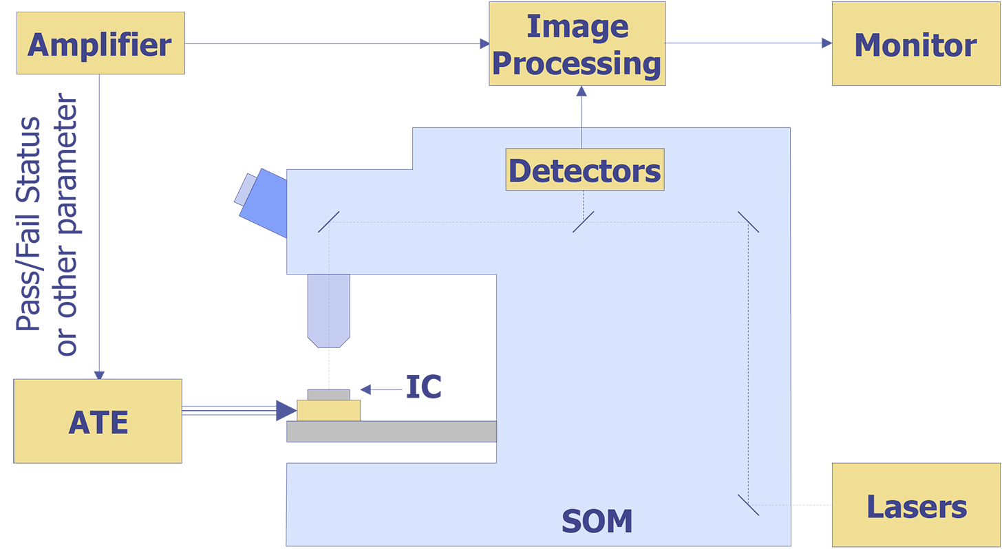
Soft Defect Localization involves probing the IC and looking for operational changes while exercising the IC. The basic diagram is shown below.


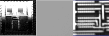
As an example, one might be looking for the reason why a circuit works at lower frequencies, but not at higher frequencies. One would set up a vector set that produces the failing condition. One would then lower the frequency to the point where the circuit just begins to pass, or just above it. By probing with an infrared wavelength laser (e.g. 1340nm), the heat from the laser might slow down the transistor in the area of the problem just enough to push it from failing to passing, or vice-versa. One can turn the laser scan into an image representing pass/fail as a function of beam position on the die. This provides a way to localize a problem that would otherwise be very difficult to do. An example of this type of image is shown below.


Soft Defect Localization is typically performed from the backside, so it occurs after the IC backside has been exposed. One generates stronger signals from a thinned die, so thinning the sample to 100 microns or less is also completed first. In some instances, using an anti-reflective coating can help produce a better image as well. SDL also requires considerable characterization of the problem during electrical test, so this work should be performed before decapsulation and backside sample preparation to ensure that one can repeatedly produce the failing condition and the passing condition. The IC must remain functional, so care must be taken to ensure the sample remains functional during the destructive sample preparation process.