System Maintenance occurs every Friday.

Optical Examination 2

Are you looking for more information regarding this and other subjects? Look no further than Semitracks' Online Training. Semitracks' Online Training contains short courses and other material useful for any Engineer trying to learn new subjects or brush up on old ones.

What is Optical Examination After Deprocessing?

Chemical deprocessing of ICs reveals physical defects related to the circuit's observed failure mode. After each deprocessing step, the die is carefully examined for defects and anomalies potentially related to the failure mode. Optical examination of the deprocessed die involves the use of a high-power optical microscope to locate, image, and photograph defects.

Why Perform Optical Examination After Deprocessing?

Optical examination is performed after each deprocessing step to locate defects related to the device failure.

How is Optical Examination After Deprocessing Performed?

Chemical deprocessing of the IC is first performed as described in Deprocessing. Optical examination is then performed after each deprocessing step by using a high power optical microscope to inspect the die for anomalies. Inspection is begun at a fairly low magnification (50X) and increased up to 500X as necessary to locate anomalies. Based on electrical or other test data, you will know what part of the die to concentrate on.

When is Optical Examination After Deprocessing Performed?

Optical examination after deprocessing is performed immediately following each deprocessing step to examine the die for anomalies. Optical examination is generally performed during deprocessing to ensure that the layer being etched has been completely removed. Optical examination is non-destructive and should be performed prior to SEM imaging, which leaves a carbon residue on areas that have been imaged.

References on Optical Examination After Deprocessing

  1. Microelectronics Failure Analysis Techniques: A Procedural Guide, compiled and edited by Ed Doyle, Jr., Rome Air Development Center, Griffiss AFB, NY, and Bill Morris, General Electric Company, Syracuse, NY.
  2. John R. Devaney, Gerald L. Hill, and Robert G. Seippel, Failure Analysis, Mechanisms, Techniques, and Photo Atlas, Failure Recognition and Training Services, Inc., Monrovia, CA, 1983.
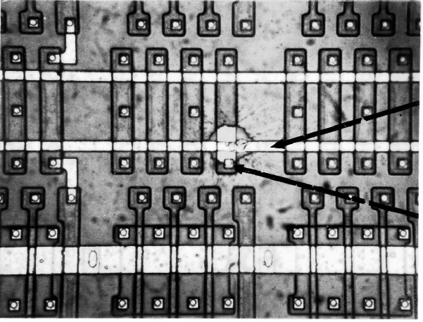
Photograph of a masking defect is shown at low magnification (200X). (Courtesy Sandia Labs) Photograph of a masking defect is shown at low magnification (200X). (Courtesy Sandia Labs)
Figure 1. Photograph of a masking defect is shown at low magnification (200X). (Courtesy Sandia Labs)
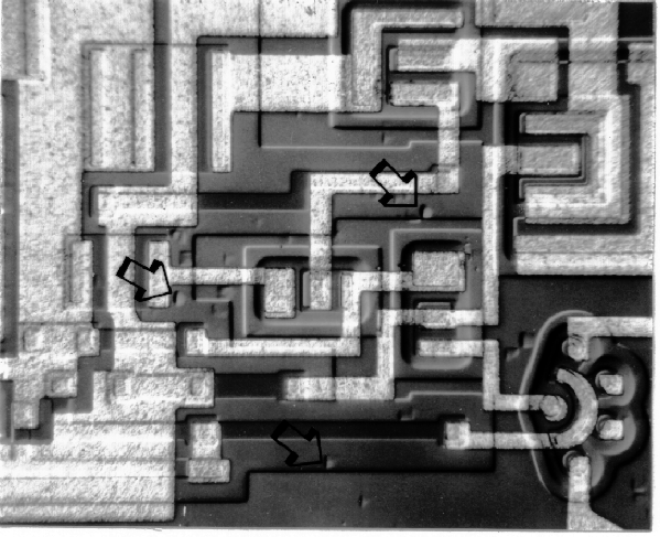
Photograph of a masking defect at higher magnification (1000X). (Courtesy Sandia Labs) Photograph of a masking defect at higher magnification (1000X). (Courtesy Sandia Labs)
Figure 2. Photograph of a masking defect at higher magnification (1000X). (Courtesy Sandia Labs)
Photograph of a processing defect at higher magnification (600X). (Courtesy Sandia Labs) Photograph of a processing defect at higher magnification (600X). (Courtesy Sandia Labs)
Figure 3. Photograph of a processing defect at higher magnification (600X). (Courtesy Sandia Labs)
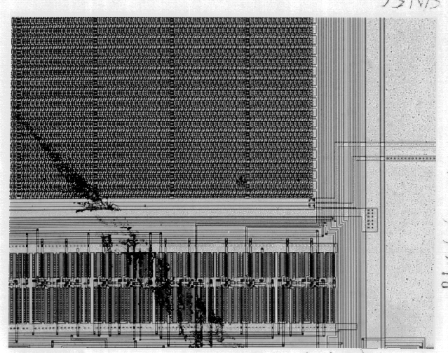
Photograph of mechanical damage is shown at low magnification (100X). (Courtesy Sandia Labs) Photograph of mechanical damage is shown at low magnification (100X). (Courtesy Sandia Labs)
Figure 4. Photograph of mechanical damage is shown at low magnification (100X). (Courtesy Sandia Labs)
Photograph of an epitaxial layer stacking fault is shown at low magnification (100X). (Courtesy DM Data) Photograph of an epitaxial layer stacking fault is shown at low magnification (100X). (Courtesy DM Data)
Figure 5. Photograph of an epitaxial layer stacking fault is shown at low magnification (100X). (Courtesy DM Data)
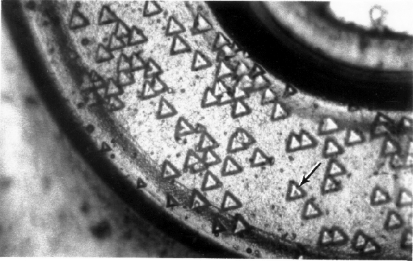
Photograph of an epitaxial layer stacking fault at high magnification (750X). (Courtesy DM Data) Photograph of an epitaxial layer stacking fault at high magnification (750X). (Courtesy DM Data)
Figure 6. Photograph of an epitaxial layer stacking fault at high magnification (750X). (Courtesy DM Data)
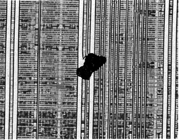
Photograph of a particle on a die surface after glass removal. (Courtesy Sandia Labs) Photograph of a particle on a die surface after glass removal. (Courtesy Sandia Labs)
Figure 7. Photograph of a particle on a die surface after glass removal. (Courtesy Sandia Labs)
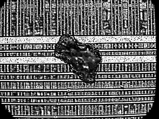
Photograph of a particle beneath the surface shown in Fig. 7 (before glass removal). (Courtesy Sandia Labs) Photograph of a particle beneath the surface shown in Fig. 7 (before glass removal). (Courtesy Sandia Labs)
Figure 8. Photograph of a particle beneath the surface shown in Fig. 7 (before glass removal). (Courtesy Sandia Labs)