System Maintenance occurs every Friday.
System Maintenance occurs every Friday.
Infrared microscopy deals with light with wavelengths in the 0.7 µm to 2.0 µm range of the electromagnetic spectrum. Under these lighting conditions, most common semiconductor materials are transparent. Figure 1 shows the transparency of Si, GaAs, and Ge as a function of wavelength. In silicon, for example, radiation at wavelengths longer than 1.12 µm (silicon's bandgap at 300 K is 1.12 eV) does not have enough energy to excite valence band electrons into the conduction band, therefore silicon appears transparent to these wavelengths.
Microscopy in the infrared region is identical to microscopy in the visible region. All types of illumination, including bright field, dark field, and Nomarski interference contrast, are possible. The types of glass used in most microscopes conveniently passes IR light, but some objectives have coatings which filter it out. Special lenses that have been optimized for IR work are available. Usually, light sources are fitted with heat absorbing filters that filter out radiation at wavelengths longer than 1.0µm. These filters must be removed and a silicon filter must be added (this filter blocks out visible light) to allow only IR illumination of the specimen. Once the proper illumination has been obtained, some form of IR to visual converter must be used to allow viewing of the IR images. Two types of converters are common: S1 photocathodes, which are used as "eyepieces" and TV cameras with IR sensitive vidicon tubes. These converters work on the principle of having the IR photon flux converted into an electron flux, which strikes a phosphor coating without changing its cross-sectional distribution.
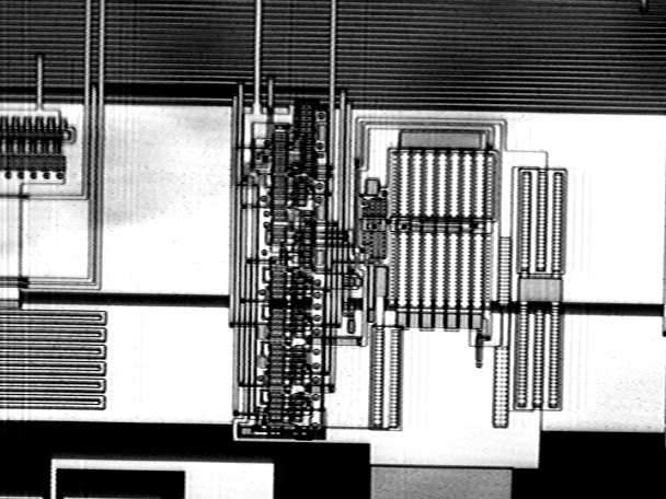
While both transmitted and reflected modes of operation, like optical microscopy, are possible, the work on ICs is primarily done in reflected mode, as the IC is usually in some type of package. Some work is done looking through the back of the die after it has been polished. This type of work allows imaging of the wire bonds and inspection for problems like corrosion in plastic packaged parts; however, it requires destructive sample preparation. In general, any irregularity that creates a change in the material, such as a large change in doping, crystalline defect, or alignment between layers can be imaged. Also, events like CMOS latchup can be imaged as forward biased junctions emit a small amount of radiation from electron hole pair recombination that is in the near-IR region.
The only major drawback to IR microscopy is its spatial resolution. In microscopy, the maximum resolution is usually one to two times the illuminating wavelength. For IR radiation, resolutions around 1-2µm are typical. The lack of resolution may limit the usefulness of IR microscopy on sub-micron technologies.
Basically, there are two reasons to use IR backside imaging. First, if the metal layers are so dense that the layers underneath them cannot be imaged adequately and removal of those upper layers is inappropriate. Backside IR work can be done, with adequate care taken, without altering the electrical operation of the IC. Second, if the IC is packaged active side down in flip chip technologies, IR backside imaging would be less destructive than frontside optical examination of the IC.
Aside from the above instances, if corrosion of the bond pads is suspected on a plastic encapsulated IC, it can be difficult to examine without questioning whether or not the decapsulation process itself caused the corrosion. To prove that decapsulation did not cause the corrosion, the package can be polished from the backside, allowing the bond pads to be examined from the backside. In doing this, the condition of the metal on the bond pads can be assessed without disturbing the plastic on top of them and exposing the bond pad metal to any corrosive chemicals.
Aside from sample preparation, IR backside imaging is almost as easy to do as frontside optical examination, with the exception that the human eye cannot directly see the images. The most commonly used method is to use an IR-sensitive camera and to watch images on a video monitor. Most standard optical microscopes can be outfitted with a silicon filter in front of the light source (to block out the visible light) and an IR-sensitive camera system. More recently, the use of IR lasers on scanning optical microscope systems has allowed users to switch from visible light imaging to IR imaging at the touch of a button.
Since this type of imaging relies on the transparency os semiconductor materials in order to work, transmitted IR light images can be formed. However, in general, transmitted IR imaging is seldomly useful on ICs. As such, IR backside imaging on ICs will almost always be done in reflected mode.
The most obvious scenario to apply IR backside imaging is when the top side of the IC is not accessible, as in flip chip technologies. For these technologies, IR backside imaging requires less destructive sample preparation than frontside examination, which requires removing the IC. A second example is when the interconnect layers on the IC are too dense to effectively see through and removing the upper layers is not yet justifiable. In this situation, IR backside imaging can allow inspection of the IC without losing electrical functionality. Other examples include instances where corrosion of bond pads is suspected and removal of the plastic packaging material would create questions about whether the plastic package removal process corroded the bond pads. The package can be polished away from the backside to allow inspection of the bond pads from the backside without ever exposing the frontside to a corrosive environment.