Are you looking for more information regarding this and other subjects? Look no further than Semitracks' Online Training. Semitracks' Online Training contains short courses and other material useful for any Engineer trying to learn new subjects or brush up on old ones.
What is a High Power Examination?
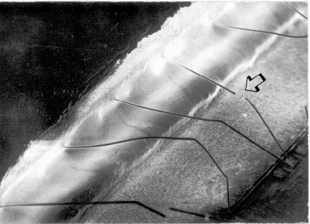
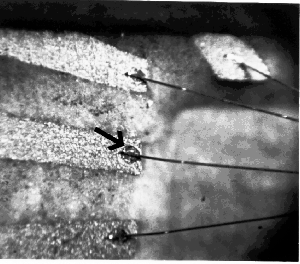
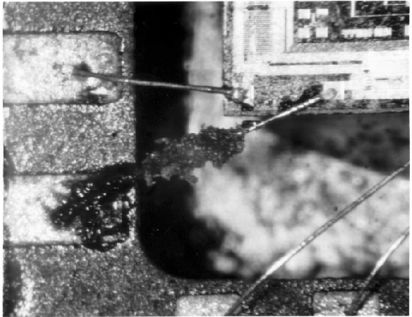
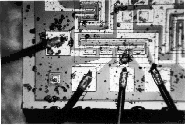
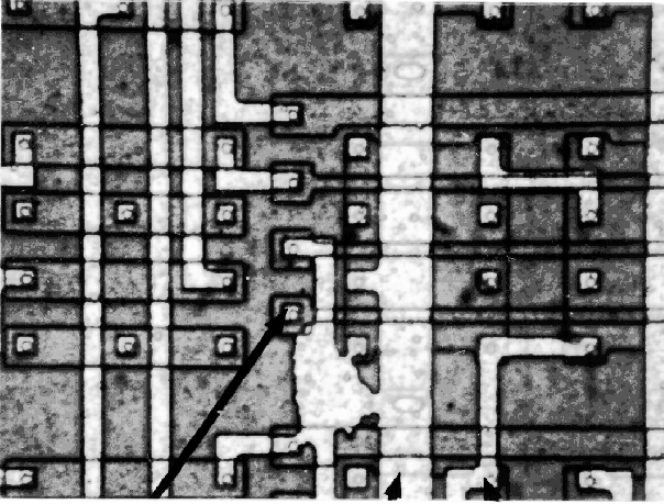
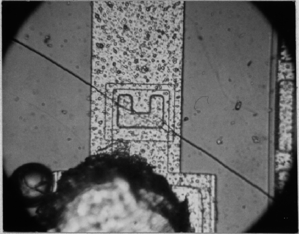
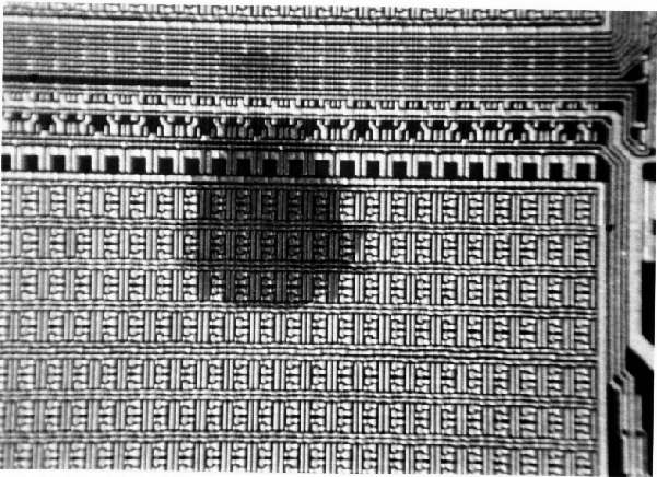
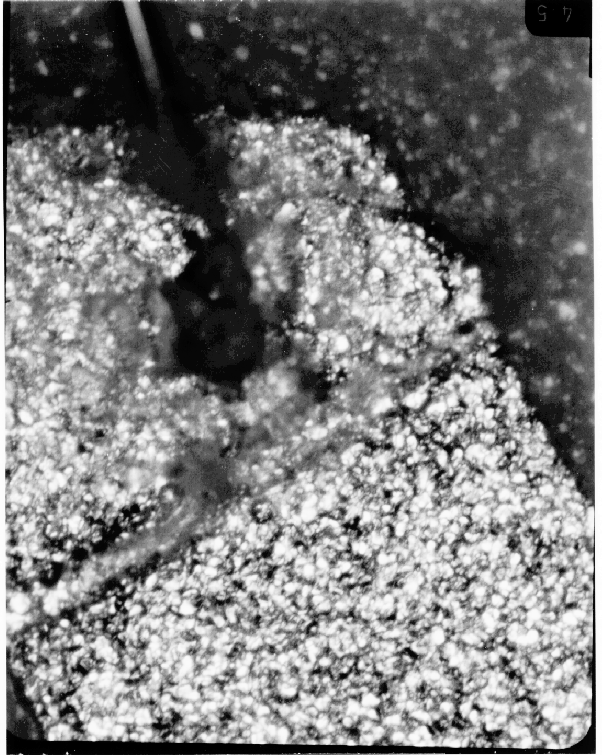
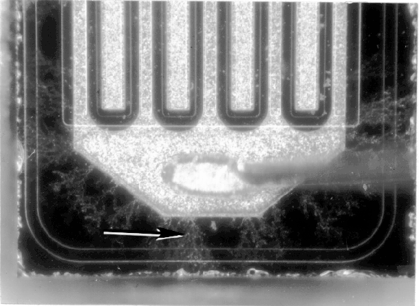
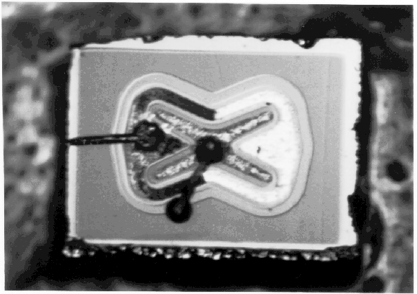
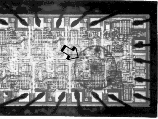
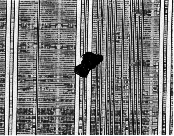
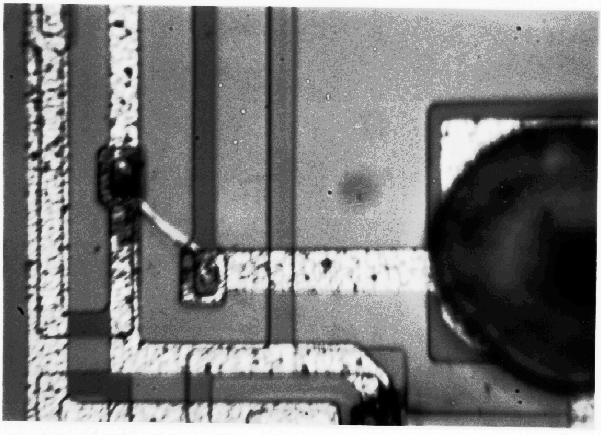
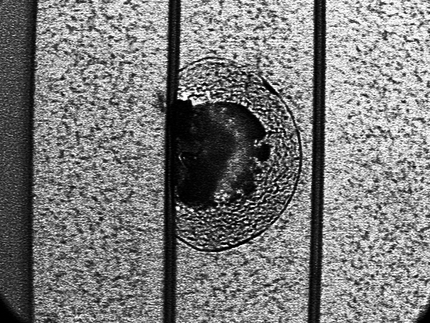
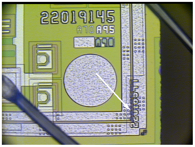
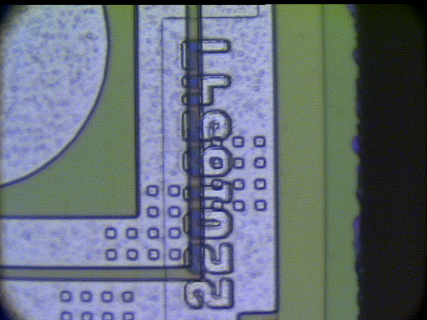
Arguably the most versatile and powerful technique available to the failure analyst, high power examination is generally regarded as optical examination using a magnification range of 50X up to the wavelength limitations of visible light (approximately 2000X). Optical microscopes that use reflected light are the most common pieces of equipment used for performing a high power examination. A number of failure modes in ICs can be detected by examining the IC at high magnifications using an optical microscope.
An optical microscope system consists of three main components: the magnification system, the light source, and the sample stage. The magnification system can be sub-divided into the objective lenses, the field lens, and the eyepiece.
The objective lenses fall into three categories: achromatic, apochromatic, or non-achromatic. Achromatic lenses are corrected for two colors, normally red and green. Apochromatic lenses are corrected for three colors, normally red, green, and violet. Non-achromatic lenses are not corrected for any colors; this means they yield color halos in the formed image. In addition, lenses have a specific magnifying power, numerical aperture rating, and focal length.
The field lens is the lens installed in the column of the microscope between the objective and the eyepiece. Some microscopes come with adjustable field lenses allow several differing magnifications to be placed in front of the objective.
The eyepiece can be either a negative (Huggenian), positive (Ramsden), or true negative (Amplifying) lens. Several types of light sources are available for use with optical microscopes: low voltage tunsten filament lamps, zenon, mercury vapor lamps, and cesium-iodide lamps. Each has a slightly different color temperature, yielding different color balances. Most stages for failure analysis purposes are regular (non-inverted) stages.
Why Perform a High Power Examination
Accurately diagnosing and precisely locating failure mechanisms and defects in CMOS ICs are often difficult tasks. Many techniques are available, but successful failure analysis requires careful selection of these techniques and the sequencing of their use. Nondestructive techniques are usually preferred if they are easy to implement and have a high probability of success. Optical microscopy has several desirable attributes, including high spatial sensitivity, simple sample preparation, and absence of special environmental requirements.
How is a High Power Examination Performed?
The device to be examined is placed under the optical microscope with the proper lighting and its surface is examined. High power examination can be performed on any suitable metallurgical microscope. These microscopes are available from a number of vendors and possess numerous configurations and options. The three most useful modes of examination are light field, dark field and interference contrast. Be sure to avoid hitting the die with the microscope objective, as this can damage both the IC and the objective.
When is a High Power Examination Performed?
Due to its benign effect on the device and potential for uncovering useful information, High Power Examination is often used for CMOS ICs after a low power examination of the IC.
MIL STD Procedures for Internal Visual (MIL-STD 883C Method 2010.7)
1. Purpose. The purpose of this test is to check the internal materials, construction, and workmanship of microcircuits for compliance with the requirements of the applicable procurement document. This test will normally be used prior to capping or encapsulation on a 100 percent inspection basis to detect and eliminate devices with internal defects that could lead to device failure in normal application. It may also be employed on a sampling basis prior to capping to determine the effectiveness of the manufacturer's quality control and handling procedures for microelectronic devices. Complex microcircuits may require substitution of alternate screening procedures for visual inspection criterion pertaining to metal coverage, oxide, and diffusion faults that are difficult or impractical to perform. These alternate screening methods and procedures are documented in Method 5004, and their use shall be on an optional basis. Test condition A provides a rigorous and detailed procedure for internal visual inspection intended for high reliability class S microcircuits. Test condition B provides procedures for internal visual inspection intended for classes B and C microcircuits (classes of microcircuits refer to screening requirements of Method 5004).
2. Apparatus. The apparatus for this test shall include optical equipment capable of the specified magnification(s) and any visual standards (gages, drawings, photographs, etc.) necessary to perform an effective examination and enable the operator to make objective decisions as to the acceptability of the device being examined. Adequate fixturing shall be provided for handling devices during examination to promote efficient operation without inflicting damage to the units.
3. Procedure
- General. The device shall be examined in a suitable sequence of observations within the specified magnification range to determine compliance with the requirements of the applicable procurement document and the criteria of the specified test condition. For nonJAN devices if a specified visual inspection requirement is in conflict with circuit design topology or construction, it shall be documented and specifically approved by the procuring activity. For JAN devices there shall be no waivers. The inspections and criteria in this method shall be required inspections for all devices and locations to which they are applicable. Where the criterion is intended for a specific device process or technology, it has been indicated.
- Sequence of inspection. The order in which criteria are presented is not a required order of examination and may be varied at the discretion of the manufacturer. Visual criteria specified in 3.1.1.2, 3.1.1.5, 3.1.1.7, 3.1.2, 3.1.7 e and f, 3.1.8, 3.1.9 a through d, and 3.2.1.2, 3.2.1.5, 3.2.1.7, 3.2.2, 3.2.7 e and f, 3.2.8, 3.2.9 a, b, and d may be examined prior to die attachment without required reexamination after die attachment. Visual criteria specified in 3.1.6.2, 3.1.6.3, 3.2.6.2, and 3.2.6.3 may be examined prior to bonding without reexamination after bonding. Visual criteria specified in 3.2.1.1 and 3.2.3 may be examined prior to die attachment at "high magnification" provided they are reexamined after die attachment at "low magnification." When inverted mounting techniques are employed, the inspection criteria contained herein that cannot be performed after mounting shall be conducted prior to attachment of the die. Devices which fail any test criteria herein are defective devices, regardless whether or not the observation is made at the scheduled observation station, and the defective device shall be rejected and removed at the time of observation.
- Inspection control. In all cases, examination prior to final preseal inspection shall be performed under the same quality program that is required at the final preseal inspection station. Care shall be exercised after inspections per 3 b, to insure that defects created during subsequent handling will be detected and rejected at final preseal inspection. During the time interval between visual inspection and preparation for sealing, devices shall be stored in a controlled environment. Devices examined to 3.1 criteria shall be inspected and prepared for sealing in a class 100 environment and devices examined to 3.2 criteria shall be inspected and prepared for sealing in a class 100,000 environment per Federal Standard 209, except that the maximum allowable relative humidity in either environment shall not exceed 65 percent. Devices shall be in covered containers when transferred from one controlled environment to another.
- Magnification. "High magnification" inspection shall be performed perpendicular to the die surface with the device under illumination normal to the die surface. "Low magnification" inspection shall be performed with either a monocular, binocular, or stereomicroscope, and the inspection performed within an angle of 30 degrees from the perpendicular to the die surface with the device under suitable illumination. The inspection criteria of 3.1.4, 3.2.4, and 3.2.6.1 may be examined at "high magnification" at the manufacturer's option.
- Reinspection. When inspection for product acceptance or quality verification of the visual requirements herein is conducted subsequent to the manufacturer's successful inspection, the additional inspection may be performed at any magnification specified by the applicable test condition, unless a specific magnification is required by the procurement document. Where sampling is used rather than 100 percent reinspection, 6.4 of MIL-M-38510 shall apply.
- Exclusions. Where conditional exclusions have been allowed, specific instruction as to the location and conditions for which the exclusion can be applied shall be documented in the assembly inspection drawing.
- Definitions:
- Active circuit area includes all areas of functional circuit elements, operating metallization or any connected combinations thereof excluding beam leads.
- Controlled environment shall be in accordance with the requirements of Federal Standard 209 class 100 environment for air cleanliness and humidity, except that the maximum allowable relative humidity shall not exceed 50 percent. If an inert gas environment such as nitrogen is used to satisfy the requirements for storing in a controlled environment the above stated requirement apply.
- Diffusion tub is an isolated volume of semiconductor material, either "P" or "N" type, surrounded by isolation material.
- Foreign material is defined as any material that is foreign to the microcircuit or any non-foreign material that is displaced from its original or intended position within the microcircuit package and shall be considered attached when it cannot be removed by a nominal gas blow (approximately 20 psig). Conductive foreign material is defined as any substance that appears opaque under those conditions of lighting and magnification used in routine visual inspection. Particles shall be considered embedded in the glassivation when there is evidence of color fringing around the periphery of the particle.
- Functional circuit elements are diodes, transistors, crossunders, capacitors, and resistors.
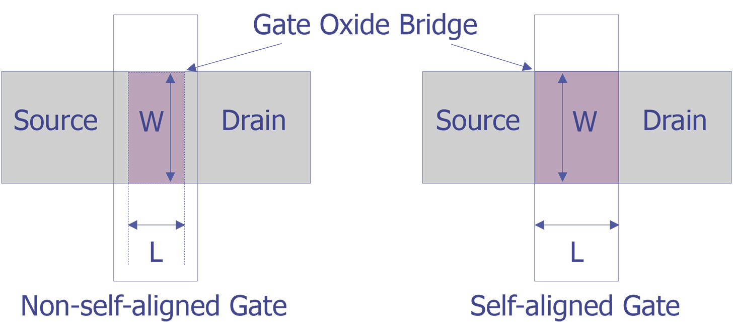
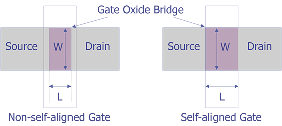
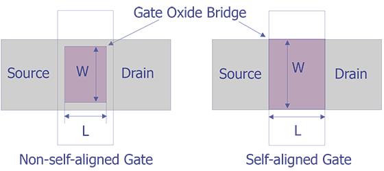
- Gate oxide bridge is the area lying between the drain and source diffusions of MOS structures. References to the metallization covering the gate oxide bridge shall include all materials that are used for the gate electrode.
- Glassivation is the top layer(s) of transparent insulating material that covers the active circuit area including metallization, except bonding pads and beam leads. Crazing is the presence of minute cracks in the glassivation.
- Junction is the outer edge of a passivation step that delineates the boundary between "P" and "N" type semiconductor material.
- Multilayered metallization (conductors) is two or more layers of metal or any other material used for interconnections that are not isolated from each other by a grown or deposited insulating material. The term "underlying metal" shall refer to any layer below the top layer of metal.
- Multilevel metallization (conductors) is two or more layers of metal or any other material used for interconnections that are isolated from each other by a grown or deposited insulating material.
- Operating metallization (conductors) is all metal or any other material used for interconnection except metallized scribe lines, test patterns, unconnected functional circuit elements, unused bonding pads, and identification markings.
- Organic polymer (epoxy) vapor residue is the material that is emitted from the polymer, that forms on an available surface.
- Original width is the width dimension or distance that is intended by design (e.g., original metal width, original diffusion width, original beam width, etc.,).
- Passivation step is a change in thickness of the passivation for metal to metal or metal to silicon interconnection, by design, excluding lines on the surface where passivation layers have been removed as a result of normal device processing.
- Passivation is the silicon oxide, nitride or other insulating material that is grown or deposited directly on the die prior to the deposition of metal.
- Peripheral metal is all metal that lies immediately adjacent to or over the scribe grid.
- Thick film is that conductive/resistive/dielectric system that is a film having greater than 50,000 angstroms thickness.
- Thin film is that conductive/resistive/dielectric system that is a film equal to or less than 50,000 angstroms in thickness.
- Substrate is the supporting structural material into and/or upon which the passivation, metallization and circuit elements are placed.
- Narrowest resistor width is the narrowest portion of a given resistor prior to trimming however, the narrowest resistor width for a block resistor may be specified in the approved manufacturer's design documentation.
- Kerf is that portion of the resistor area from which resistor material has been removed or modified by trimming.
- Detritus is fragments of original or laser modified resistor material remaining in the kerf.
- Block resistor is a sheet resistor which for purposes of trimming is designed to be much wider than would be dictated by power density requirements and shall be identified in the approved manufacturer's precap visual implementation document.
- Interpretations. For inspections performed in the range of 75X to 100X, the criteria of "0.1 mil of passivation, separation, or metal" can be satisfied by a "line of separation" or a "line of metal." Reference herein to "that exhibits" shall be considered satisfied when the visual image or visual appearance of the device under examination indicates a specific condition is present and shall not require confirmation by any other method of testing. When other methods of test are to be used for confirming that a reject condition does not exist, they shall be approved by the procuring activity.
3.1 Test condition A. Internal visual examination as required in 3.1.1 through 3.1.6 shall be conducted on each microcircuit and each integrated circuit chip. In addition, the applicable criteria contained in 3.1.7 through 3.1.9 shall be used for the appropriate microcircuit areas where glassivation, dielectric isolation or film resistors are used. The "high magnification" inspection shall be within the range of 100X to 200X, the "low magnification" within the range of 30X to 60X.
3.1.1 Metallization defects "high magnification." No device shall be acceptable that exhibits the following defects in the operating metallization:
3.1.1.1 Metallization scratches. A scratch is any tearing defect including probe marks in the surface of the metallization:
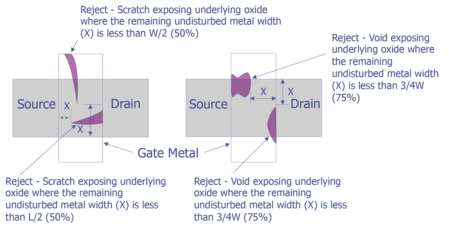
- Scratch in the metallization excluding bonding pads and beam leads that leaves less than 50 percent of the original metal width undisturbed (see Figure 23).
- Scratch in the metallization over a passivation step that leaves less than 75 percent of the original metal width at the step undisturbed.
- Scratch in the bonding pad or fillet area that reduces the metallization path width connecting the bond to the interconnecting metallization to less than 50 percent of the narrowest entering interconnect metallization stripe width. If two or more stripes enter a bonding pad, each shall be considered separately.
- Scratch in the metallization, over the gate oxide bridge (see Figure 25) (applicable to MOS structures).
- Scratch in multilayered metallization excluding bonding pads and beam leads that exposes underlying metal or passivation anywhere along its length and leaves less than 75 percent of the original metal width undisturbed (see Figure 23).
- Scratch(es) (probe mark(s), etc.,) in the bonding pad area that exposes underlying passivation over more than 25 percent of the original unglassivated metallization area.
3.1.1.2 Metallization voids. A void is any region in the metallization where underlying metal or passivation is visible that is not caused by a scratch.
- Void(s) in the metallization that leaves less than 75 percent of the original metal width undisturbed (see Figure 24).
- Void(s) in the metallization over the gate oxide bridge that leaves less than 75 percent of the metallization length (L) or width (W) between source and drain diffusions undisturbed (see Figure 25) (applicable to MOS structures).
- Void(s) that leave less than 75 percent of the metallization area over the gate oxide bridge undisturbed (applicable to MOS structures).
- Void(s) in the bonding pad area that leaves less than 75 percent of its original unglassivated metallization area undisturbed.
- Void(s) in the bonding pad or fillet area that reduces the metallization path width connecting the bond to the interconnecting metallization to less than 75 percent of the narrowest entering interconnect metallization stripe width (see Figure 26).
- Void(s) in the metallization area of a thin film capacitor that reduces the metallization area by more than 25 percent.
3.1.1.3 Metallization corrosion. Any metallization corrosion. Metallization having any localized discolored area shall be closely examined and rejected unless it is demonstrated to be a harmless film, glassivation interface, or other obscuring effect.
3.1.1.4 Metallization adherence. Any metallization lifting, peeling, or blistering.
3.1.1.5 Metallization probing. Criteria contained in 3.1.1.1 shall apply as limitations on probing damage.
3.1.1.6 Metallization bridging. Any metallization bridging where the separation between any two metallization paths is reduced to less than 50 percent of the original separation or 1.0 mil whichever is less. In no case shall this separation be less than 0.1 mil.
3.1.1.7 Metallization alignment.
- Contact window that has less than 75 percent of its area covered by metallization.
- Contact window that has less than a continuous 50 percent of its perimeter covered by metallization.
- Contact window that has less than 75 percent of its perimeter on two adjacent sides covered by metallization (applicable to MOS structures).
NOTE: When by design, metal is completely contained in a contact window or does not cover the entire contact perimeter, criteria 3.1.1.7 b and c perimeter coverage can be deleted.
- A metallization path not intended to cover a contact window that is separated from the window by less than 0.25 mil. When this requirement exceeds 50 percent of the original separation, the minimum separation shall be 0.1 mil.
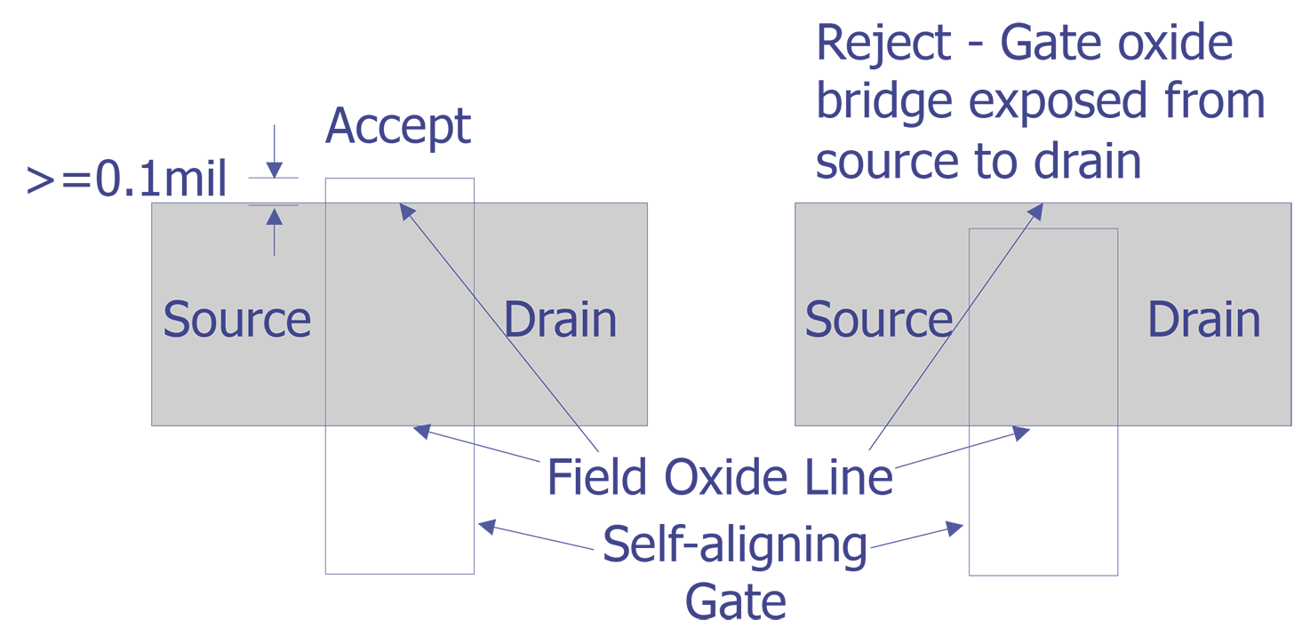
- Any exposure of the gate oxide bridge from source to drain diffusion (applicable to MOS structure) (see Figure 27).
- Any exposure of the gate oxide bridge that leaves less than 75 percent of the metallization coincident with the source and drain diffusion junction line undisturbed (applicable to MOS structures).
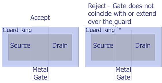
- Gate metallization not coincident with or extending over the diffused guard ring.
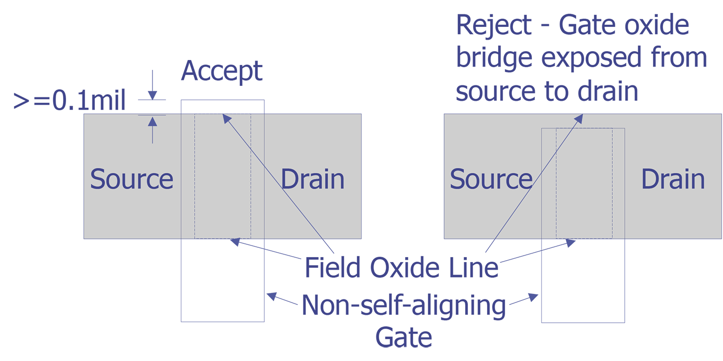
NOTE: Criteria 3.1.1.7 g applies to MOS structures containing a diffused guard ring. MOS devices that do not have a diffused guard ring shall have gate metallization extending not less than 0.1 mil beyond the gate oxide bridge (see Figure 28 and Figure 29 and Figure 30).
3.1.2 Diffusion and passivation layer(s) faults "high magnification." No device shall be acceptable that exhibits the following:
3.1.2.1 Diffusion faults:
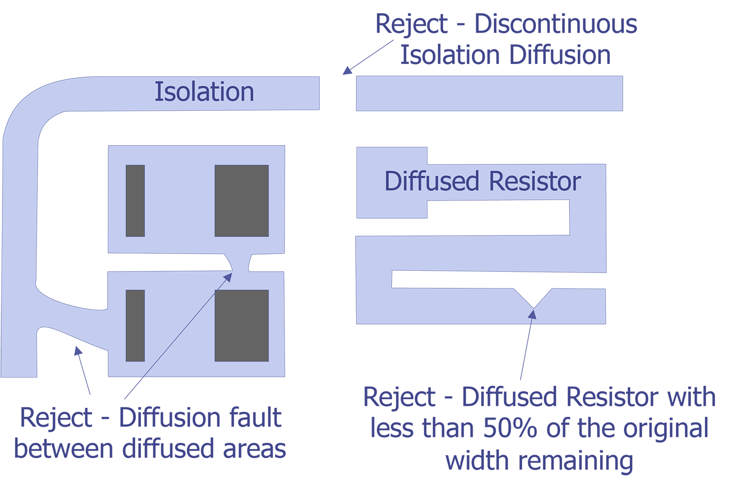
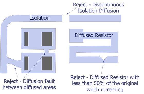
- Any diffusion fault that allows bridging between diffused areas (see Figure 31).
- Any isolation diffusion that is discontinuous or any other diffused area with less than 25 percent (50 percent for resistors) of the original diffusion width that remains (see Figure 31).
3.1.2.2 Passivation faults:
- Either multiple lines or a complete absence of passivation visible at the edge and continuing under the metallization (see Figure 32).
NOTE: Double or triple lines at the edge of the defect indicate it can have sufficient depth to penetrate down to bare silicon.
- Active junction not covered by passivation, unless by design.
- Contact window that extends across a junction, unless by design.
3.1.3 Scribing and die defects "high magnification." No device shall be acceptable that exhibits:
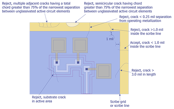
- Less than 0.25 mil of passivation visible between operating metallization or bond periphery and edge of the die.
NOTE: Criteria of 3.1.3 a can be excluded for beam leads and peripheral metallization including bonding pads where the metallization is at the same potential as the die.
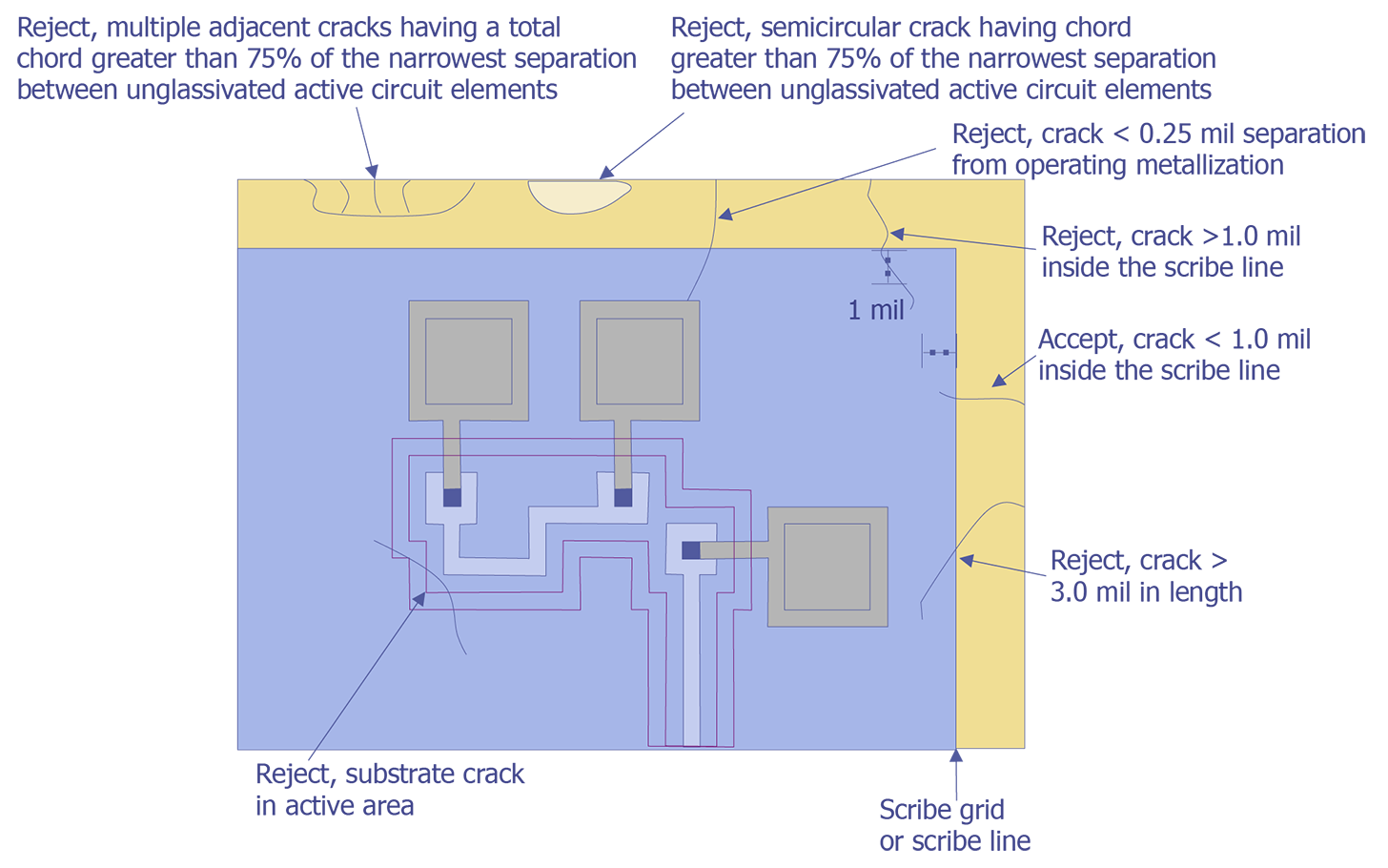
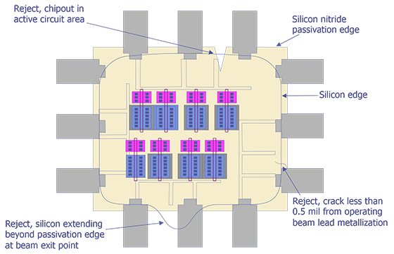
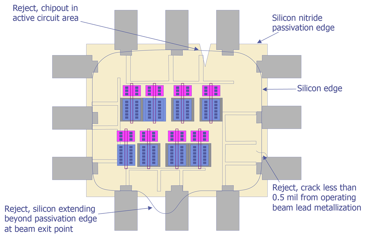
- A chipout or crack in the active circuit area (see Figure 33).
- A crack that exceeds 3.0 mil in length or comes closer than 0.25 mil to any operating metallization, or other functional circuit element (see Figure 33 and Figure 34).
- Semicircular crack or multiple adjacent cracks, terminating at the die edge whose chord is equal to or greater than 75 percent of the narrowest separation between unglassivated active circuit elements (see Figure 33).
NOTE: Operating metallization, scribe line and bond wires shall be considered active circuit elements.
- Exposed silicon extending over the passivation edge at the point or the beam lead exit from the die (see Figure 34) (applicable to beam lead structures).
- Die having attached portions of the active circuit area of another die.
- A crack that exceeds 1.0 mil in length inside the scribe grid, scribe line, or silicon edge for beam lead devices that point toward operating metallization or functional circuit elements.
NOTE: Criteria of 3.1.3 b, c, and h can be excluded for beam lead devices where the chip-out or crack does not extend into the silicon material.
- A crack that comes closer than 0.5 mil to operating beam lead metallization (see Figure 34).
3.1.4 Bond inspection "low magnification." This inspection and criteria shall be the required inspection for the bond type(s) and location(s) to which they are applicable when viewed from above.
NOTE: Wire tail is not considered part of the bond when determining physical bond dimensions (see Figure 35).
3.1.4.1 Gold ball bonds. No device shall be acceptable that exhibits:
- Gold ball bonds on the die or package post wherein the ball bond diameter is less than 2.0 times or greater than 5.0 times the wire diameter.
- Gold ball bonds where the wire exit is not completely within the periphery of the ball.
- Gold ball bonds where the wire center exit is not within the boundaries of the bonding pad.
- Intermetallic formation extending radially more than 0.1 mil completely around the periphery of any gold ball bond for that portion of the gold ball bond located on metal.
3.1.4.2 Wedge bonds. No device shall be acceptable that exhibits:
- Ultrasonic wedge bonds on the die or package post that are less than 1.2 times or more than 3.0 times the wire diameter in width, or are less than 1.5 times or more than 5.0 times the wire diameter in length (see Figure 36).
- Thermocompression wedge bonds on the die or package post that are less than 1.5 times or more than 3.0 times the wire diameter in width or are less than 1.5 times or more than 5.0 times the wire diameter in length (see Figure 36).
3.1.4.3 Tailless bonds (crescent). No device shall be acceptable that exhibits:
- Tailless bonds on the die or package post that are less than 1.2 times or more than 5.0 times the wire diameter in width, or are less than 0.5 times or more than 3.0 times the wire diameter in length (see Figure 36).
- Tailless bonds where bond impression does not cover the entire width of the wire.
3.1.4.4 General (gold ball, wedge, and tailless). As viewed from above, no device shall be acceptable that exhibits:
- Bonds on the die where less than 75 percent of the bond is within the unglassivated bonding pad area.
- Wire bond tails that extend over or make contact with any metallization not covered by glassivation and not connected to the wire.
- Wire bond tails that exceed two wire diameters in length.
- Bonds on the package post that are not completely within two package post width (i.e. narrowest post width) from the inner edge of the package post or bonds that are not completely within the boundaries of the package post.
- Rebonding.
- Bonds placed so that the separation between bonds is less than 1.0 mil, excluding bonds connected by a common connector.
- Bonds placed so that the separation between the bond and unglassivated metallization not connected to it is less than 1.0 mil. Where such requirements exceed the minimum unglassivated metal spacing and for glassivated metallization, the minimum separation between the bond and glassivated or unglassivated metallization not connected to it shall not be less than 0.25 mil.
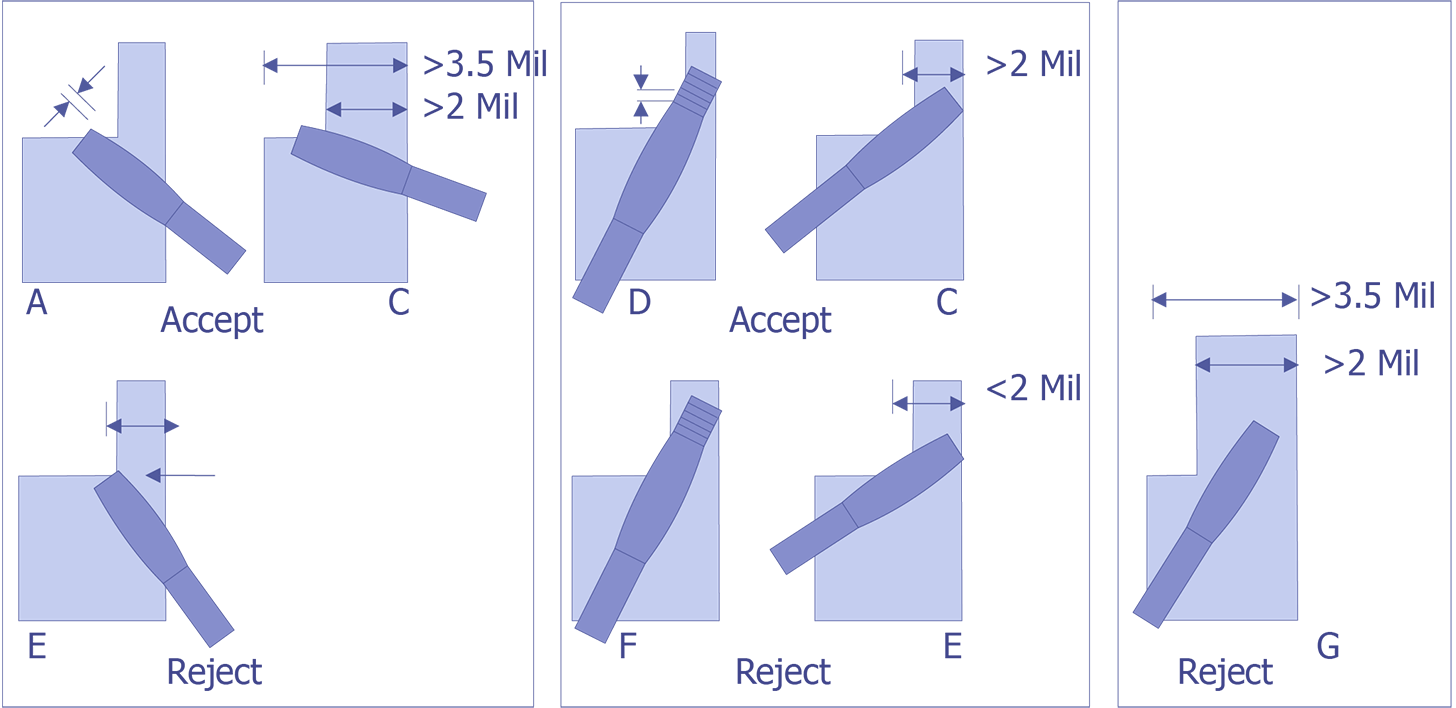
- Bonds at the point where metallization exits from the bonding pad that do not exhibit a line of undisturbed metallization visible between the periphery of the bond and at least one side of the entering metallization (see Figure 37 and Figure 38 and Figure 39).
NOTE: Criteria 3.1.4.4 h can be excluded when the entering metallization strip is greater than 2.0 mils in width and the bond pad dimension on the entering metal stripe side is greater than 3.5 mils.
- Bonds where more than 25 percent of the bond is located in an area containing die preform mounting material.
- Bonds placed so that the wire exiting from the bond crosses over another bond.
- Any evidence of rebonding or repair of conductors by bridging with or addition of bonding wire or ribbon.
3.1.4.5 Beam lead. This inspection and criteria shall apply to the completed bond area made using either direct tool contact or a compliant intermediate layer. No device shall be acceptable that exhibits:
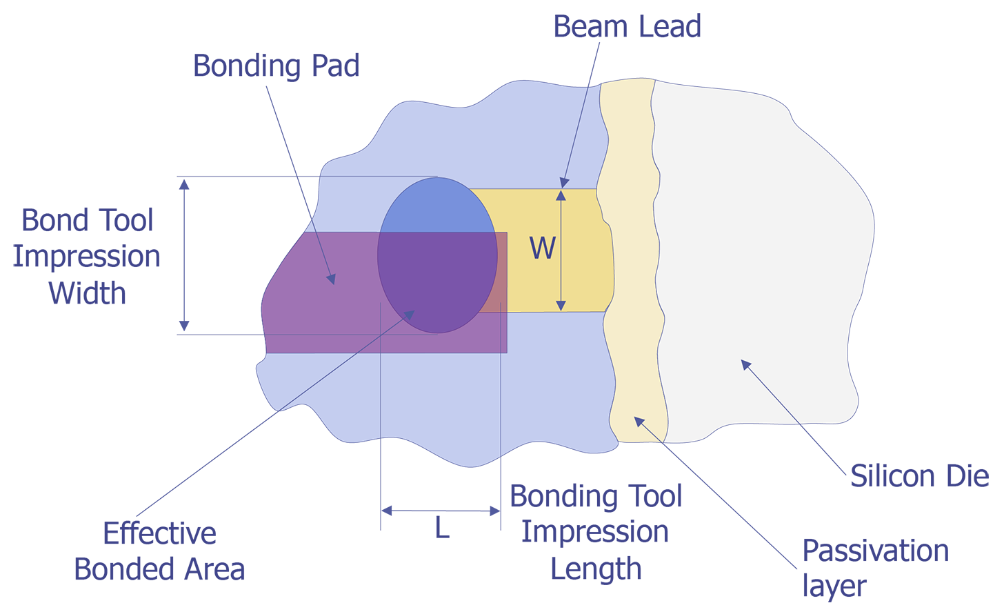
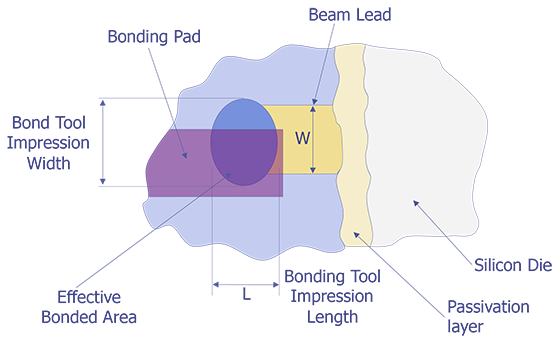
- Bonds where the tool impression does not completely cross the entire beam width.
- Bonds on thin film substrate metal where the tool impression increases the beam lead width less than 15 percent (10 percent for compliant bonds) or greater than 75 percent of the undeformed beam width.
- Bonds where the tool impression length is less than 1.0 mil (see Figure 18).
- Bonding tool impression less than 1.0 mil from the die edge (see Figure 41).
- Effective bonded area less than 50 percent of that which would be possible for an exactly aligned beam (see Figure 40).
- Cracks or tears in the effective bonded area of the beam greater than 50 percent of the original beam width.
- Bonds placed so that the separation between bonds and between bonds and operating metallization not connected to them is less than 0.1 mil.
- Bonds lifting or peeling.
3.1.5 Internal leads "low magnification." This inspection and criteria shall be required inspection for the lead type(s) and location(s) to which they are applicable when viewed from above. When the requirement of 3.1.5.1a is not easily determined vertically, then the device may be rotated about the X and Y axis to allow a horizontal view of the wires such that the vertical separation is verified.
3.1.5.1 Wires. No device shall be acceptable that exhibits:
- Any wire that comes closer than two wire diameters to unglassivated operating metallization, another wire (common wires excluded), package post, unpassivated die area (except for wires or pads which are at the die or substrate potential), or any portion of the package, including the plane of the lid to be attached.
NOTE: Within a 5.0 mils spherical radial distance from the perimeter of the bond on the die surface, the separation can be 1.0 mil. Use of a stereomicroscope to assure approximately 1.0 mil of clearance (i.e. absolute measurement are not practical in a production environment) shall be acceptable to satisfy this requirement.
- Nicks, bends, cuts, crimps, scoring, or neckdown in any wire that reduces the wire diameter by more than 25 percent.
- Missing or extra lead wires.
- Tearing at the junction of the wire and bond.
- Any wire making a straight line run from die bonding pad to package post that has no arc.
- Wire(s) crossing wire(s), except common conductors.
- Wire(s) not in accordance with bonding diagram.
3.1.5.2 Beams. No device shall be acceptable that exhibits the following:
- Voids, nicks, depressions, or scratches that leave less than 50 percent of the beam width undisturbed.
- Beam separation from the die.
- Missing or partially fabricated beam leads unless by design.
- Beam leads that are not bonded.
- Bonded area closer than 0.1 mil to the edge of the passivation layer.
- Less than 0.1 mil passivation layer between the die and the beam visible at both edges of the beam (see Figure 34 and Figure 37).
3.1.6 Package conditions (magnification as indicated). No device shall be acceptable that exhibits:
3.1.6.1 Foreign material. All foreign material or particles may be blown off with a nominal gas blow (approximately 20 psig). The device shall then be inspected and be rejected when it exhibits the following:
- NOTE: Die inspections shall be at "high magnifications" while package and lid inspection may be at "low magnifications."
- Foreign particle(s) on the surface of the die or within the package or on the lid or cap that is large enough to bridge the narrowest spacing between unglassivated operating material (metallization, bare silicon, mounting material, bonding wire, etc).
NOTE: Silicon chips shall be considered as foreign particles.
- Embedded foreign particles on the die that bridge two metallization paths.
- Liquid droplets, chemical stains or photoresist on the die surface that bridge any combinations of unglassivated metal or bare silicon areas.
- d. Ink on the surface of the die that covers more than 25 percent of a bonding pad area or that bridges any combination of unglassivated metallization or bare silicon areas.
NOTE: As an alternative to 100 percent visual inspection of lids or caps per the criteria of 3.1.6.1 a, the lids or caps may be subjected to a suitable cleaning process and quality verification approved by the qualifying activity (procuring activity for nonJAN) provided the lids or caps are subsequently held in a controlled environment until capping or preparation for seal.
3.1.6.2 Die mounting "low magnification."
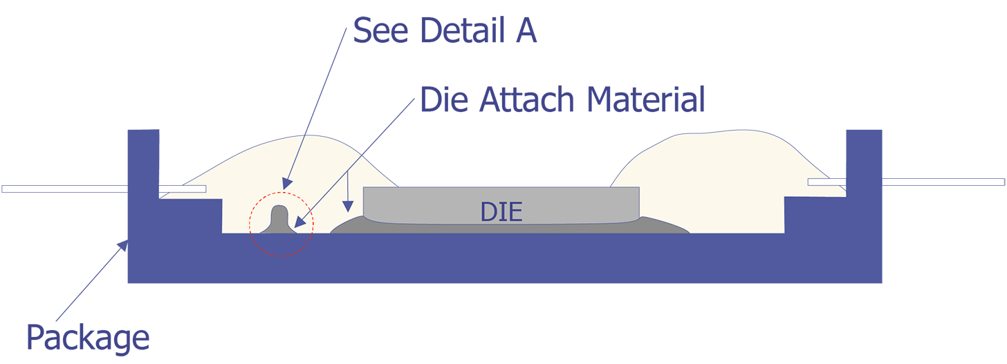
- Die mounting material buildup that extends onto the top surface of the die or extends vertically above the top surface of the die.
- Die to header mounting material not visible around at least two complete sides or 75 percent of the die perimeter, except for transparent die.
- Transparent die with less than 50 percent of the area bonded.
- Flaking of the die mounting material.
- Balling or buildup of the die mounting material that does not exhibit a fillet beginning at the maximum radius of the ball and completely surrounding it when viewed from above.
3.1.6.3 Die orientation. Die not located or oriented in accordance with the applicable assembly drawing of the device.
- Die not located or oriented in accordance with the applicable assembly drawing of the device.
- Die not level within 10 degrees with respect to the package cavity.
3.1.7 Glassivation defects, "high magnification." No device shall be acceptable that exhibits:
- Glass crazing or glass damage that prohibits the detection of visual criteria contained herein.
- Any lifting or peeling of the glassivation.
- Two or more adjacent active metallization paths not covered by glassivation, excluding bonding pad cutouts.
- Unglassivated areas greater than 5.0 mils in any dimension, unless by design.
- Unglassivated areas at the edge of bonding pad exposing silicon.
- Glassivation covering more than 25 percent of the bonding pad area.
- Crazing over a film resistor.
- Scratches in the glassivation that disturb metal and bridge metallization paths.
- Cracks (not crazing) in the glassivation that form a closed loop over adjacent metallization paths.
- Glassivation voids that expose any portion of a thin film resistor or fusible link except for polycrystalline silicon links where the glassivation is opened by design.
3.1.8 Dielectric isolation "high magnification." No device shall be acceptable that exhibits:
- A discontinuous isolation line (typically a black line) around each diffusion tub containing functional circuit elements.
- Absence of a continuous isolation line between any adjacent tubs, containing functional circuit elements.
- A diffused area which overlaps dielectric isolation material and comes closer than 0.1 mil to an adjacent diffusion tub; or an overlap of more than one diffusion area into the dielectric isolation material (see Figure 42 and Figure 43).
- A contact window that touches or overlaps dielectric material.
- Metallization scratch and void defects over a dielectric isolation step shall be in accordance with criteria contained in 3.1.1.1. b and 3.1.1.2.a.
3.1.9 Film resistor, "high magnification." Rejection shall be based on defects found within the actively used portions of the film resistor. Metallization defect criteria of 3.1.1 shall apply. No device shall be acceptable that exhibits:
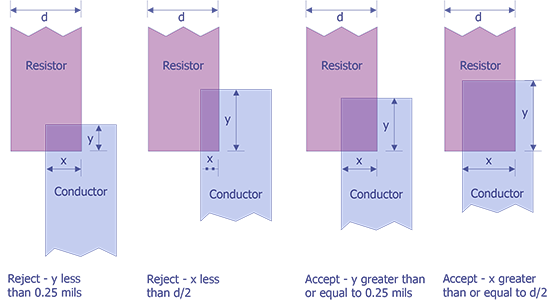
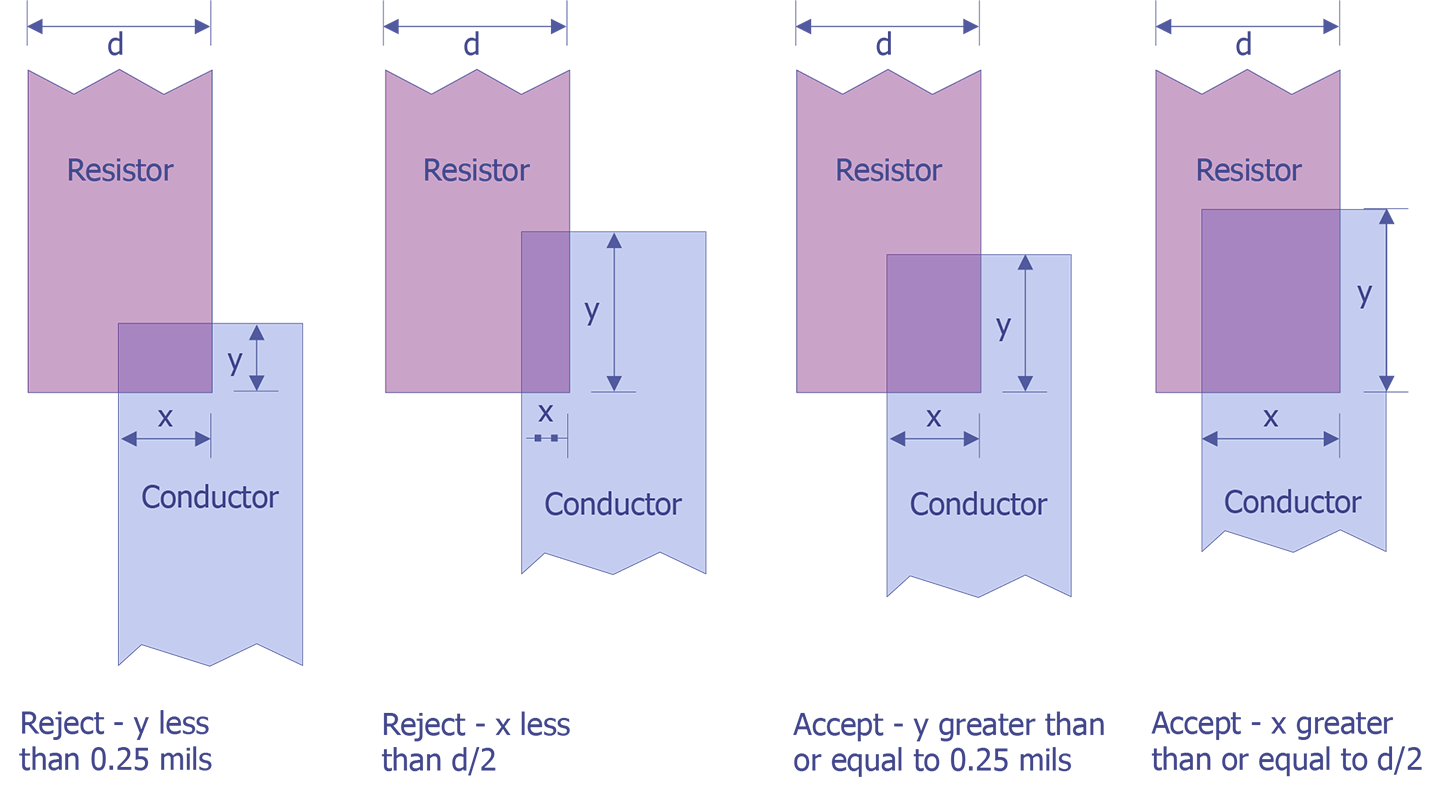
- Any misalignment between the conductor/resistor in which the actual width X of the overlap is less than 50 percent of the original resistor width (see Figure 44).
- Contact overlap between the metallization and film resistor in which the length dimension Y is less than 0.25 mil (see Figure 45).
- Increase in resistor width greater than 25 percent of the original width.
- Necking down that reduces the width of film resistor material at a terminal.
- Void that leaves less than 75 percent of the film resistor undisturbed at a terminal.
- Any sharp change in color of resistor material within 0.1 mil of the resistor/connector termination.
- Inactive resistor inadvertently connected to two separate points on an active circuit.
- Separation between any two resistors or a resistor and a metallization path that is less than 0.25 mil.
- Any thin film resistor that crosses a substrate irregularity (e.g., dielectric isolation line, oxide/diffusion step, etc.).
- Any resistor width less than 0.25 mil or one half the narrowest resistor width, whichever is greater, resulting from voids or scratches or a combination thereof (see Figure 81).
3.1.10 Laser trimmed thin film resistors, "high magnification". Rejection shall be based on defects found within the actively used portions of the film resistor. No device shall be acceptable that exhibits:
- A kerf less than 0.1 mil in width.
NOTE: Criteria does not apply for edge trimming.
- A kerf containing particles of detritus.
- A kerf containing untrimmed resistor material, unless that material is continuous across the kerf, and is undisturbed for a width greater than 1/2 times the narrowest resistor width or 0.25 mil, whichever is greater (see Figure 80).
- Resistor width that has been reduced by trimming to less than 1/2 the narrowest resistor width or 0.25 mil, whichever is greater, including voids, scratches, or a combination thereof, in the trim area (see Figure 82 and Figure 83).
- Trim path into the metallization, except for block resistors.
NOTE: Conductors or resistors may be trimmed open for link trims or by design.
- Trim for block resistors which extends into the metallization (excluding bonding pads) more than 25 percent of the original metal width (see Figure 84).
- Pits into the silicon dioxide in the kerf which do not exhibit a line of separation between the pit and the resistor material.
3.2 Test condition B. Internal visual examination as required in 3.2.1 through 3.2.6 shall be conducted on each microcircuit and each integrated circuit chip. In addition, the applicable criteria in 3.2.7 through 3.2.9 shall be used for the appropriate microcircuits areas where glassivation, dielectric isolation or film resistors are used. The "high magnification" inspection shall be performed within the range of 75X to 150X and the "low magnification" within the range of 30X to 60X.
3.2.1 Metallization defects "high magnification." No device shall be acceptable that exhibits the following in the operating metallization.
3.2.1.1 Metallization scratches. A scratch is any tearing defect, including probe marks in the surface of the metallization:
- Scratch in the metallization excluding bonding pads, that exposes underlying passivation anywhere along its length and leaves less than 50 percent of the original metal width undisturbed (see Figure 46).
- Scratch that completely crosses a metallization path and damages the surface of the surrounding passivation or glassivation on either side. (For MOS devices, the path shall be the (L) dimension (see Figure 49).
- Scratch in multilayered metallization that exposes the underlying metal anywhere along its length and leaves less than 25 percent of the top-layer original metal width undisturbed (see Figure 47).
NOTE: Criteria of 3.2.1.1 a, b and c can be excluded for peripheral power or ground metallization where parallel paths exist such that an open at the scratch would not cause an unintended isolation of the metallization path. When application of this exclusion causes or permits a device design to exceed the current density limitation imposed by the procurement document, this exclusion shall not apply. Current density shall be determined by design not visual inspection.
- Scratch in the metallization over a passivation step that leaves less than 75 percent of the original metal width at the step undisturbed.
NOTE: Criteria of 3.2.1.1 a through d can be excluded for the last 25 percent of linear length of the contact cut and all metal beyond on the termination end(s) of the metallization runs. In these cases there shall be at least 50 percent of the contact opening area covered by metallization and at least a continuous 40 percent of the contact opening perimeter covered by undisturbed metallization (see Figure 48).
- Any scratch in the metallization, over the gate oxide bridge, that exposes underlying passivation and leaves less than 50 percent of the length or width of the metallization between source and drain diffusion undisturbed (see Figure 50) (applicable to MOS structures).
- Scratch in the metallization that exposes the dielectric material of a thin film capacitor or crossover.
- Scratch in the bonding pad or fillet area that exposes underlying passivation and reduces the metallization path width connecting the bond to the interconnecting metallization to less than 50 percent of the narrowest entering interconnect metallization stripe width. If two or more stripes enter a bonding pad, each shall be considered separately.
- Scratch(es) (probe mark(s), etc.,) in the bonding pad area that exposes underlying passivation over more than 25 percent of the original unglassivated metallization area.
3.2.1.2 Metallization voids. A void is any defect in the metallization where underlying metal or passivation is visible and is not caused by a scratch.
- Void(s) in the metallization that leaves less than 50 percent of the original metal width undisturbed (see Figure 51).
NOTE: Criteria of 3.2.1.2 a can be excluded for peripheral power or ground metallization where parallel paths exist so that an open at the void(s) would not cause an unintended isolation of the metallization path. When application of this exclusion causes or permits a device design to exceed the current density limitation imposed by the procurement document, this exclusion shall not apply. Current density shall be determined by design, not visual inspection.
- Void(s) in the metallization over a passivation step that leaves less than 75 percent of the original metal width at the step undisturbed.
NOTE: Criteria of 3.2.1.2 a and b can be excluded for the last 25 percent of linear length of the contact cut and all metal beyond on the termination end(s) of metallization runs. In these cases there shall be at least 50 percent of the contact opening area covered by metallization and at least a continuous 40 percent of the contact opening perimeter covered by undisturbed metallization (see Figure 48).
- Void(s) in the metallization over the gate oxide bridge that leaves less than 75 percent of the metallization length (L) between source and drain diffusions undisturbed (see Figure 50) (applicable to MOS structures).
- Void(s) that leave less than 60 percent of the metallization area over the gate oxide bridge undisturbed (applicable to MOS structures).
- Void(s) that leaves less than 75 percent of the metallization width coincident with the source or drain diffusion junction line, undisturbed (see Figure 50) (applicable to MOS structures).
- Void(s) in the bonding pad area that leaves less than 75 percent of its original unglassivated metallization area undisturbed.
- Void(s) in the bonding pad or fillet area that reduces the metallization path width connecting the bond to the interconnecting metallization to less than 50 percent of the narrowest entering interconnect metallization stripe width (see Figure 53).
NOTE: If two or more stripes enter a bonding pad, each shall be considered separately.
- Void(s) in the metallization of a thin film capacitor that reduces the metallization area by more than 25 percent.
3.2.1.3 Metallization corrosion. Any metallization corrosion.
3.2.1.4 Metallization adherence. Any metallization lifting, peeling, or blistering.
3.2.1.5 Metallization probing. Criteria contained in 3.2.1.1 shall apply as limitations on probing damage.
3.2.1.6 Metallization bridging. Any metallization bridging where the separation between any two metallization paths is reduced to less than 0.1 mil, unless by design.
3.2.1.7 Metallization alignment.
- Contact window that has less than 50 percent of its area covered by metallization.
- Contact window that has less than 40 percent of its perimeter covered by metallization.
NOTE: When, by design, metal is completely contained in a contact window or does not cover the entire contact perimeter, criteria 3.2.1.7 a. area coverage, or 3.2.1.7 b. perimeter coverage, can be deleted as applicable provided the design criteria is satisfied.
- A metallization path not intended to cover a contact window that is separated from the window by less than 0.1 mil.
- Any exposure of the gate oxide bridge from source to drain diffusions (see Figure 54) (applicable to MOS structures).
- Any exposure of the gate oxide bridge that leaves less than 75 percent of the metallization coincident with the source and drain diffusion junction line undisturbed (applicable to MOS structures).
- Gate metallization not coincident with or extending over the diffused guard ring.
NOTE: Criteria 3.2.1.7 f applies to MOS structures containing a diffused guard ring. MOS devices that do not contain a diffused guard ring shall have gate metallization extending not less than 0.1 mil beyond the gate oxide bridge (see Figure 50 and Figure 56).
3.2.2 Diffusion and passivation layer(s) faults, "high magnification." No device shall be acceptable that exhibits the following:
- A diffusion junction line that unintentionally crosses another diffusion junction line (see Figure 57).
- Any isolation diffusion that is discontinuous (except isolation walls around unused areas or bonding pads) or any other diffused area with less than 25 percent of the original diffusion width remaining.
- Either multiple lines or a complete absence of passivation visible at the edge and continuing under the metallization (see Figure 58).
NOTE: Double or triple lines indicate that it can have sufficient depth to penetrate down to bare silicon; however, should the absence of glassivation in the defect area or the characteristics of the glassivation present allow verification of the presence or absence of passivation by color or color comparisons, respectively, then these techniques may be used. Criteria of 3.2.2 c can be excluded when a second passivation layer is applied in a separate operation prior to metallization deposition.
- An active junction not covered by passivation, unless by design.
3.2.3 Scribing and die defects, "high magnification." No device shall be acceptable that exhibits:
- Less than 0.1 mil of passivation visible between operating metallization or bond periphery and edge of the die.
NOTE: Criteria of 3.2.3 a can be excluded for beam leads and peripheral metallization including bonding pads where the metallization is at the same potential as the die.
- A chipout in the active circuit area (see Figure 59 and Figure 60).
NOTE: Criteria 3.2.3 b can be excluded for peripheral metallization that is at the same potential as the die. At least 50 percent undisturbed metallization width shall remain at the chip-out. except there shall be no width criteria where parallel paths exist so that an open at the chip-out would not cause an unintended isolation of the metallization path. When application of this exclusion causes or permits a device design to exceed the current density limitation imposed by the procurement document, this exception shall not apply. Current density shall be determined by design, not visual examination.
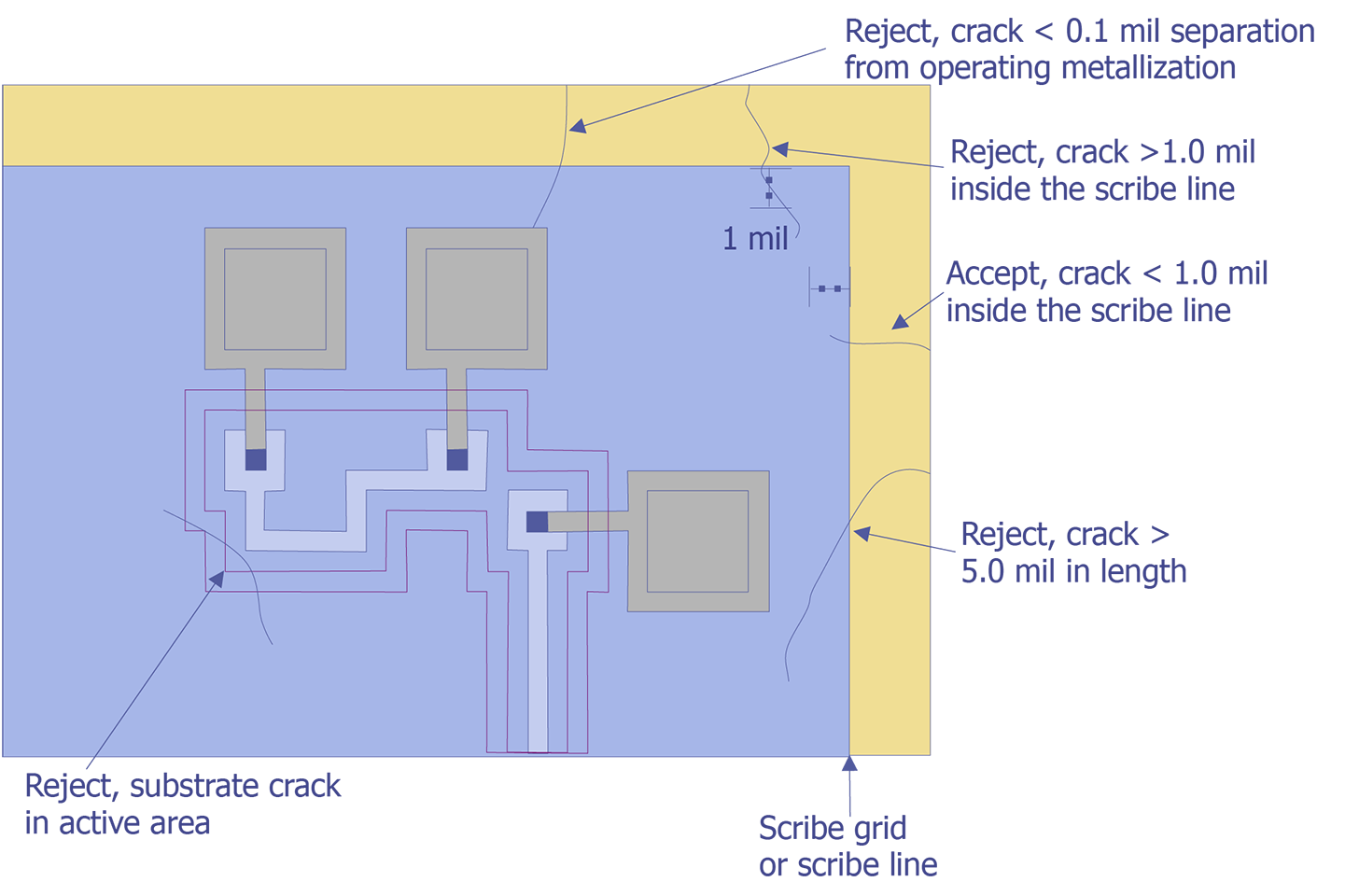
- Any substrate or passivation crack in the active circuit area or a crack that exceeds 5.0 mils in length (see Figure 59).
- Any crack that comes closer than 0.1 mil to any operating metallization or other active circuit area on the die (see Figure 59).
NOTE: Criteria of 3.2.3 d can be excluded for peripheral metallization that is at the same potential as the die.
- A crack, that exceeds 1.0 mil in length, inside the scribe grid or scribe line that points toward operating metallization or functional circuit elements (see Figure 59).
- Exposed silicon extending beyond the passivation edge at the point of the beam lead exit from the die (see Figure 60) (applicable to beam lead structures).
- A crack that comes closer than 0.5 mil to operating beam lead metallization (see Figure 60).
3.2.4 Bond inspection, "low magnification." This inspection and criteria shall be required inspection for the bond type(s) and location(s) to which they are applicable when viewed from above.
- NOTE: Wire tail is not considered part of the bond when determining physical bond dimensions.
3.2.4.1 Gold ball bonds. No device shall be acceptable that exhibits:
- Gold ball bonds on the die or package post where the ball bond diameter is less than 2.0 times or greater than 6.0 times the wire diameter.
- Gold ball bonds where the wire exit is not completely within the periphery of the ball.
- Gold ball bonds where the wire center exit is not within the boundaries of the bonding pad.
- Intermetallic formation extending radially more than 0.1 mil completely around the periphery of any gold ball bond for that portion of the gold ball bond located on metal.
3.2.4.2 Wedge bonds. No device shall be acceptable that exhibits:
- Ultrasonic wedge bonds on the die or package post that are less than 1.2 times or greater than 3.0 times the wire diameter in width, or are less than 1.5 times or greater than 5.0 times the wire diameter in length (see Figure 62).
- Thermocompression wedge bonds on the die or package post that are less than 1.5 times or greater than 3.0 times the wire diameter in width, or are less than 1.5 times or greater than 5.0 times the wire diameter in length (see Figure 62).
- Wedge bonds at the point where metallization exits from the bonding pad that do not exhibit a line of undisturbed metal visible between the periphery of the bond and at least one side of the entering metallization stripe (see Figure 63 and Figure 64 and Figure 65).
- Criteria 3.2.4.2 c can be excluded when the entering metallization strip is greater than 2.0 mils in width and the bond pad dimension on the entering metal stripe side is greater than 3.5 mils.
- The requirements of 3.2.4.2 c for visual line of metal can be satisfied when an acceptable wire tail obscures the area of concern, providing the following condition exists: Bond is located more than 0.1 mil from the intersecting line of the entering metallization stripe and the bonding pad, and there is no visual evidence of disturbed pad metallization at the bond and wire tail interface.
3.2.4.3 Tailless bonds (crescent). No device shall be acceptable that exhibits:
- Tailless bonds on the die or package post that are less than 1.2 times or greater than 5.0 times the wire diameter in width, or are less than 0.5 times or greater than 3.0 times the wire diameter in length (see Figure 62).
- Tailless bonds where the bond impression does not cover entire width of the wire.
- Tailless bonds at the point where metallization exits from the bonding pad that do not exhibit a line of undisturbed metal visible between the periphery of the bond and at least one side of the entering metallization stripe (see Figure 63).
3.2.4.4 General (gold ball, wedge and tailless). No device shall be acceptable that exhibits:
- Bonds on the die where less than 50 percent of the bond is within the unglassivated bonding pad area.
- Bonds on the package post that are not completely within two package post width (i.e. narrowest post width) from the inner edge of the package post, or bonds that are not completely within the boundaries of the package post.
- Bonds placed so that the wire exiting from the bond crosses over another bond.
- Bonds placed so that the separation between bonds or the bond and operating metallization not connected to it is less than 0.1 mil.
- Wire bond tails that extend over or make contact with any metallization not covered by glassivation and not connected to the wire.
- Wire bond tails that exceed two wire diameters in length at the bonding pad or four wire diameters in length at the package post.
- Bonds where less than 50 percent of the bond is located within an area that is free of die preform mounting material.
- A bond on top of another bond, bond wire tail or residual segment of lead wire. An ultrasonic wedge bond alongside a previous bond where the observable width of the first bond is reduced less than 0.25 mils, is considered acceptable.
- Any evidence of repair of conductors by bridging with or addition of bonding wire or ribbon.
- Any rebonding which violates the applicable rework limitations of MIL-M-38510.
3.2.4.5 Beam lead. This inspection and criteria shall apply to the completed bond area made using either direct tool contact or a compliant intermediate layer. No device shall be acceptable that exhibits:
- Bonds where the tool impression does not completely cross the entire beam width.
- Bonds on thin film substrate metal where the tool impression increases the beam lead width less than 15 percent (10 percent for compliant bonds) or greater than 75 percent of the underformed beam width.
- Bonds where the tool impression length is less than 1.0 mil (see Figure 66).
- A bonding tool impression less than 1.0 mil from the die edge (see Figure 67).
- Effective bonded area less than 50 percent of that which would be possible for an exactly aligned beam (see Figure 66).
- Cracks or tears in the effective bonded area of the beam greater than 50 percent of the original beam width.
- Bonds placed so that the separation between bonds or between bonds and operating metallization not connected to them is less than 0.1 mil.
- Bonds lifting or peeling.
3.2.5 Internal leads, "low magnification." This inspection and criteria shall be required inspection for the lead type(s) and location(s) to which they are applicable.
3.2.5.1 Wires. No device shall be acceptable that exhibits:
- Any wire that touches another: Wire (excluding common wires), package post, unglassivated operating metallization, die; or any portion of the package.
- Excessive loop or sag in any wire so that it comes closer than two wire diameters to another: Wire, package post, unglassivated operating metallization or die; or portion of the package after a spherical radial distance from the bond perimeter on the die surface of 5.0 mils for ball bonds, or 10 mils for ultrasonic and thermocompression bonds.
- Nicks, cuts, crimps, scoring, or neckdown in any wire that reduces the wire diameter by more than 25 percent.
- Attached extra wire greater than two wire diameters in length at the bonding pad or four wire diameters in length at the package post.
- Tearing at the junction of the wire and bond.
- Any wire making a straight line run from die bonding pad to package post that has no arc.
- Wire(s) crossing wire(s) (except common conductors).
- Wire(s) not in accordance with bonding diagram.
3.2.5.2 Beams. No device shall be acceptable that exhibits the following between the edge of the die and the bond are:
- Voids, nicks, depressions, or scratches that leave less than 50 percent of the beam width undisturbed.
- Beam separation from the die.
- Missing or partially fabricated beam leads, unless by design.
- Beam leads that are not bonded.
- Bonded area closer than 0.1 mil to the edge of the passivation layer.
- Lack of evidence of a passivation layer between the die and each beam (see Figure 66 and Figure 67).
3.2.6 Package conditions, "low magnification." No device shall be acceptable that exhibits:
3.2.6.1 Foreign material. All foreign material or particles may be blown off with a nominal gas blow (approximately 20 psig). The device shall then be inspected and be rejected when it exhibits the following:
- Unattached foreign material on the surface of the die or within the package.
- Unattached foreign material on the surface of the lid or cap.
NOTE: Criteria of 3.2.6.1 b can be satisfied by a nominal gas blow (approximately 20 psig) or a suitable cleaning process providing that the lids or caps are subsequently held in a controlled environment until capping.
- Attached conductive foreign material that bridges metallization paths, package leads, lead to package metallization, functional circuit elements or junctions, or any combination thereof.
- Ink on the surface of the die that covers more than 25 percent of a bonding pad area or that bridges any combination of unglassivated metallization or bare silicon areas.
3.2.6.2 Die mounting:
- Die mounting material buildup that extends onto the top surface of the die.
- Die to header mounting material not visible around at least 50 percent of the die perimeter unless it is continuous on two full nonadjacent sides of the die, except for transparent die.
- Transparent die with less than 50 percent of the area bonded.
- Flaking of the die mounting material.
- Balling or buildup of the die mounting material that does not exhibit a minimum of 50 percent peripheral fillet, when viewed from above (see Figure 69).
3.2.6.3 Die assembly. Die not located and oriented in accordance with the applicable assembly drawing of the device.
3.2.7 Glassivation defects, "high magnification." No device shall be acceptable that exhibits:
- NOTE: Criteria of 3.2.7 can be excluded when the defects are due to laser trimming. In this case, the defects outside the kerf due to laser trimming shall not be more than one half the remaining resistor width and shall leave a primary resistor path free of glassivation defects, equal to or greater than one half times the narrowest resistor width, or 0.25 mil whichever is greater (see Figure 70). A sample freeze out test shall be performed and passed when this exclusion is used. (See MIL-M-38510/210).
- Crazing that prohibits the detection of visual criteria contained herein.
- Any lifting or peeling of the glassivation.
NOTE: Lifting or peeling of the glassivation may be excluded from the criteria above, when it does not extend more than 0.001 inch distance from the designed periphery of the glassivation, provided that the only exposure of metal is of adjacent bond pads or of metallization leading from those pads.
- Two or more adjacent active metallization paths not covered by glassivation, excluding bonding pad cutouts.
- Unglassivated areas greater than 5.0 mils in any dimension, unless by design.
- Unglassivated areas at the edge of bonding pad exposing silicon.
- Glassivation covering more than 50 percent of the bonding pad area.
- Crazing over a film resistor.
- Glassivation voids that expose any portion of a thin film resistor or fusible link except for polycrystalline silicon links where the glassivation is opened by design.
3.2.8 Dielectric isolation, "high magnification." No device shall be acceptable that exhibits:
- A discontinuous isolation line (typically a black line) around each diffusion tub containing functional circuit elements (see Figure 71).
- Absence of a continuous isolation line between any adjacent tubs containing functional circuit elements.
- A diffused area which overlaps dielectric isolation material and comes closer than 0.1 mil to an adjacent diffusion tub; or an overlap of more than one diffusion area into the dielectric isolation material (see Figure 71).
- A contact window that touches or overlaps dielectric isolation material.
- Metallization scratch and void defects over a dielectric isolation step shall be in accordance with criteria in 3.2.1.1 d and 3.2.1.2 b.
3.2.9 Film resistor, "high magnification." Rejection shall be based on defects found within the actively used portions of the film resistor. Metallization defect criteria of 3.2.1 shall apply. No device shall be acceptable that exhibits the following:
- Any misalignment between the conductor/resistor in which the actual width X of the overlap is less than 50 percent of the original resistor width (see Figure 73).
- Contact overlap between the metallization and film resistor in which the length dimension Y is less than 0.25 mil (see Figure 73).
- Separation between any two resistors or a resistor and a metallization path that is less than 0.1 mil, unless by design.
- Void or necking down that leaves less than 75 percent of the film resistor width undisturbed at a terminal.
- Any sharp change in the color of resistor material, within 0.1 mil of the resistor/conductor termination.
- Inactive resistor inadvertently connected to two separate points of an active circuit.
- Any thin film resistor that crosses a substrate irregularity (e.g., dielectric isolation line, oxide/diffusion step, etc.,) (see Figure 72).
- Any resistor width less than 0.25 mil or one half the narrowest width, whichever is greater, resulting from voids or scratches or a combination there of (see Figure 74).
3.2.10 Laser trimmed thin film resistors, "high magnification". Rejection shall be based on defects found within the actively used portions of the film resistor. No device shall be acceptable that exhibits:
- A kerf less than 0.1 mil in width.
NOTE: Criteria does not apply for edge trimming.
- A kerf containing particles of detritus.
- A kerf containing untrimmed resistor material, unless that material is continuous across the kerf, and is undisturbed for a width greater than 1/2 times the narrowest resistor width or 0.25 mil, whichever is greater (see Figure 76).
- Resistor width that has been reduced by trimming to less than 1/2 the narrowest resistor width or 0.25 mil, whichever is greater, including voids, scratches, or a combination thereof, in the trim area (see Figure 75, Figure 76, Figure 77, Figure 78, and Figure 79).
- Trim path into the metallization, except for block resistors.
NOTE: Conductors or resistors may be trimmed open for link trims or by design.
- Trim for block resistors which extends into the metallization (excluding bonding pads) more than 25 percent of the original metal width (see Figure 80).
- Pits into the silicon dioxide in the kerf which do not exhibit a line of separation between the pit and the resistor material.
4. Summary. The following details shall be specified in the applicable procurement document:
- Test condition (see 3).
- Where applicable, any conflicts with approved circuit design topology or construction.
- Where applicable, gages, drawings, and photographs that are to be used as standards for operator comparison (see 2).
- Where applicable, specific magnification (see 3).
References on High Power Examination
- E. Doyle Jr. and B. Morris eds., Microelectronics Failure Analysis Techniques: A Procedural Guide, IITRI, 1980, Section III.L.1-114.
- [2] J. R. Devaney, G. L. Hill, and R. G. Seippel, Failure Analysis Mechanisms Techniques and Photo Atlas, Failure Recognition and Training Services Inc., 1983 pp. 12.1-51.
