System Maintenance occurs every Friday.
Focused ion beam (FIB) systems are capable of localized (on a scale of micrometers) removal ("cutting") and deposition ("pasting") of materials. Focused Ion Beam Cut and/or Paste refers specifically to the use of the FIB system for tasks such as 1.) Exposing underlying conductors for electrical or electron-beam probing or other analysis by localized removal of passivation; 2.) Isolating devices for electrical probing and other applications by cutting conductor lines open; 3.) Depositing probe pads for probing otherwise inaccessible lines. This generally involves both cutting (to expose the line needing to be probed) and deposition (of the probe pad and strap material). 4.) Rewiring an IC to "patch" around a defective area or to test out a design change before going into production. Again, a combination of material removal and deposition is used.
The design and operation of a FIB system are somewhat analogous to those of a scanning electron microscope (SEM). An ion column produces the energetic ions, collimates them, and focuses them on the sample surface. At present, commercial FIB systems use gallium (Ga) liquid metal ion sources, and accelerating voltages up to 30 keV are common. The ion beam is collimated and focused with a series of electrostatic lenses and apertures. As in SEM, the beam is rastered over the sample surface to image it. Unlike a SEM, the beam can also be used to remove or deposit material in the raster-scanned areas.
At present, conductive materials can be deposited by ion-beam induced decomposition of organometallic molecules on the sample surface. The organometallic species is introduced near the work surface by use of a fine nozzle which connects to a gas reservoir. The most commonly used metallic species in commercial FIBs are tungsten and platinum. Processes for depositing insulating materials are presently under development by the FIB manufacturers.
A relatively new feature in FIB systems is gas-assisted material removal and deposition. One of the limitations of material removal with a FIB system is that the material that has been sputtered away is generally redeposited around the area that is being milled. With gas-assisted material removal, a gas that volatilizes the sputtered material is introduced at the work surface. This prevents redeposition and exhausts the unwanted material through the vacuum system. Gas-assisted material removal can also be used to achieve the milling of high aspect ratio (deep) holes. It is also possible that the introduction of additional gas species may be helpful during ion-induced deposition. These issues are presently being researched.
FIB Cut and/or Paste is performed in order to remove and/or deposit material locally. It may be desirable to do so in order to expose underlying conductors for electrical or electron-beam probing or to isolate or connect conductor lines. FIB Cut and/or Paste can be used to rewire an IC, which may be done in IC failure analysis to "patch" around a defective area to determine if a given defect was the cause of the observed failure, or to test out an idea for simple design changes prior to going into production.
FIB cut and/or paste operations are performed with a focused ion beam system. The details of the approach vary with the different commercial systems, but the basic principles are:
At the present time, the commercial FIB systems can deposit a variety of conducting materials. The most common conductors used are tungsten and platinum. Processes for depositing insulating materials will soon be available. Gas-assisted material removal techniques have been developed to increase the rate of material removal and minimize the problem of redeposition of material removed during milling processes.
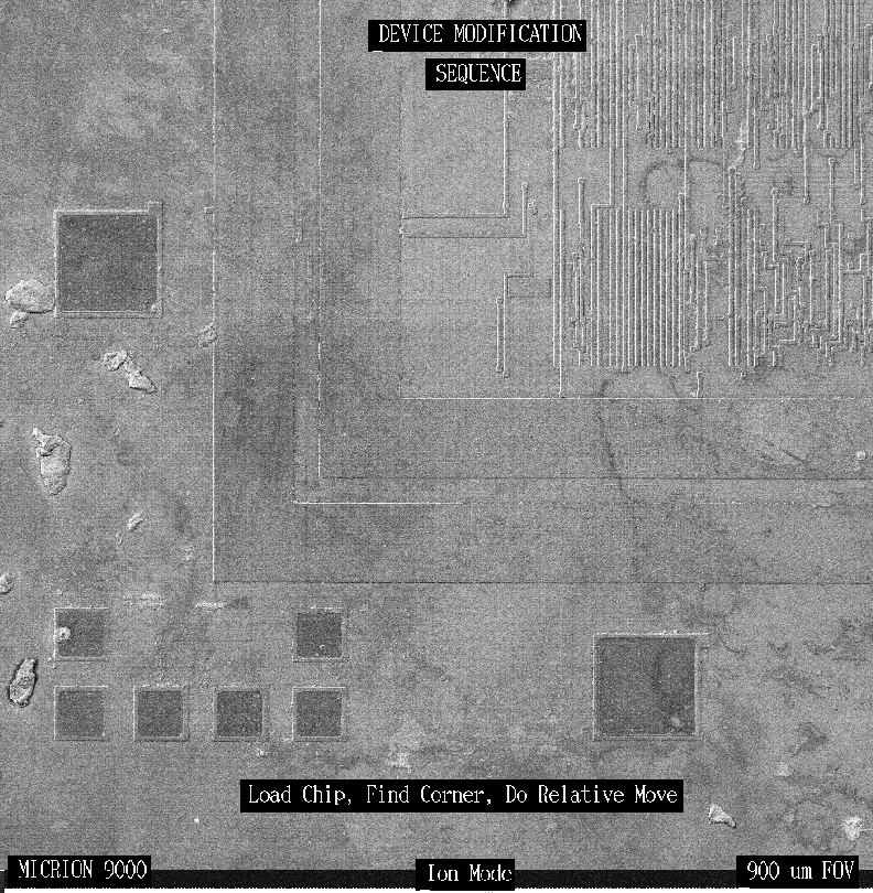
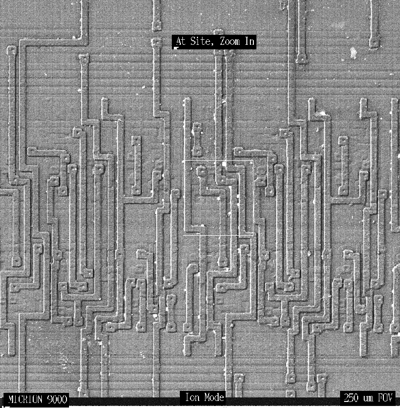
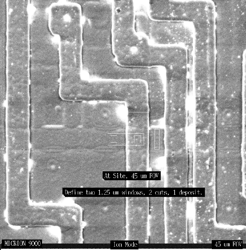
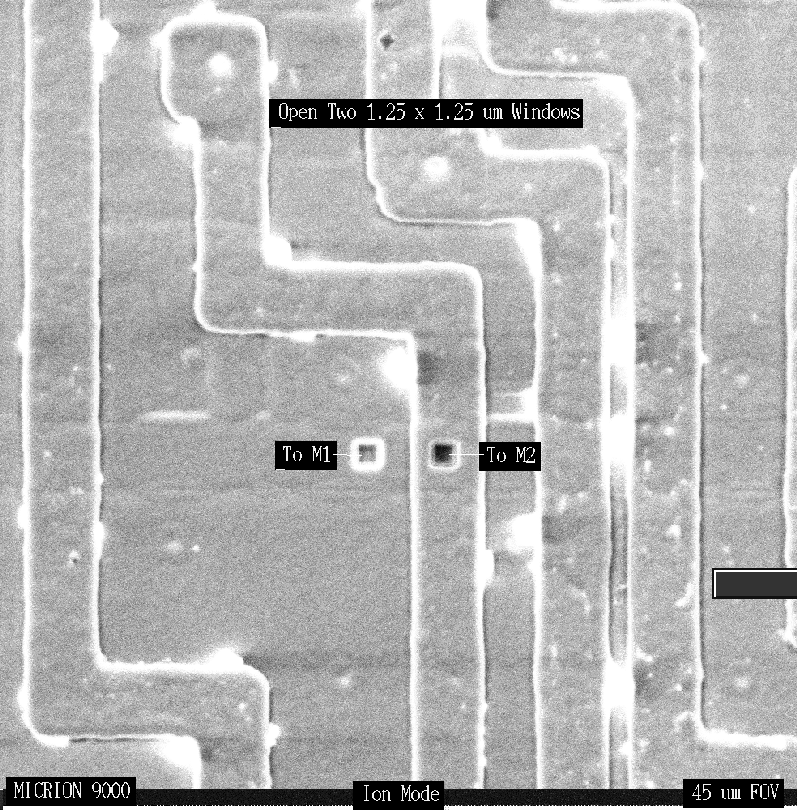
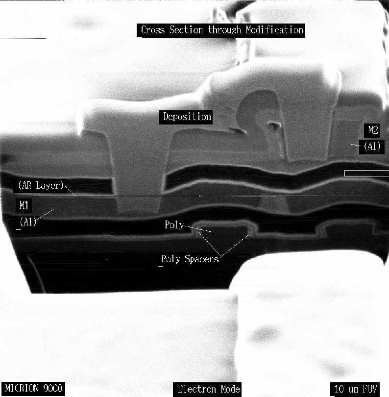
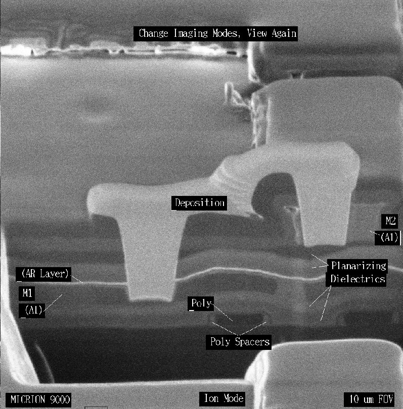
The following series of photographs (courtesy Randall G. Lee, Micrion corporation) illustrate the cut and paste (repair) sequence through pictures.
Photo 1 - Load the IC and establish coordinate system.
Photo 2 - Find the site and zoom in.
Photo 3 - Define the windows for cuts and depositions.
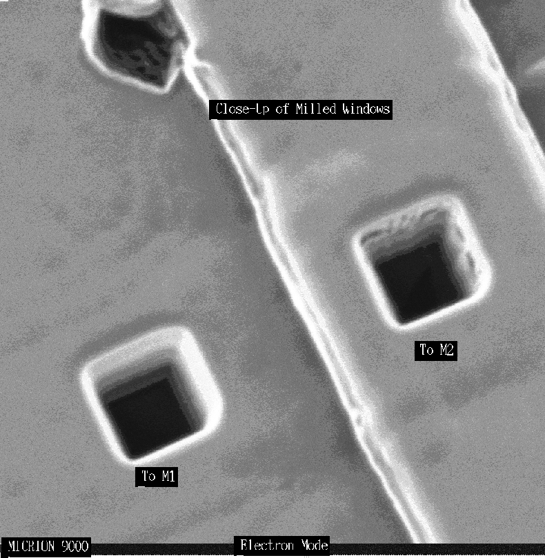
Photo 4 - Mill open the cut windows.
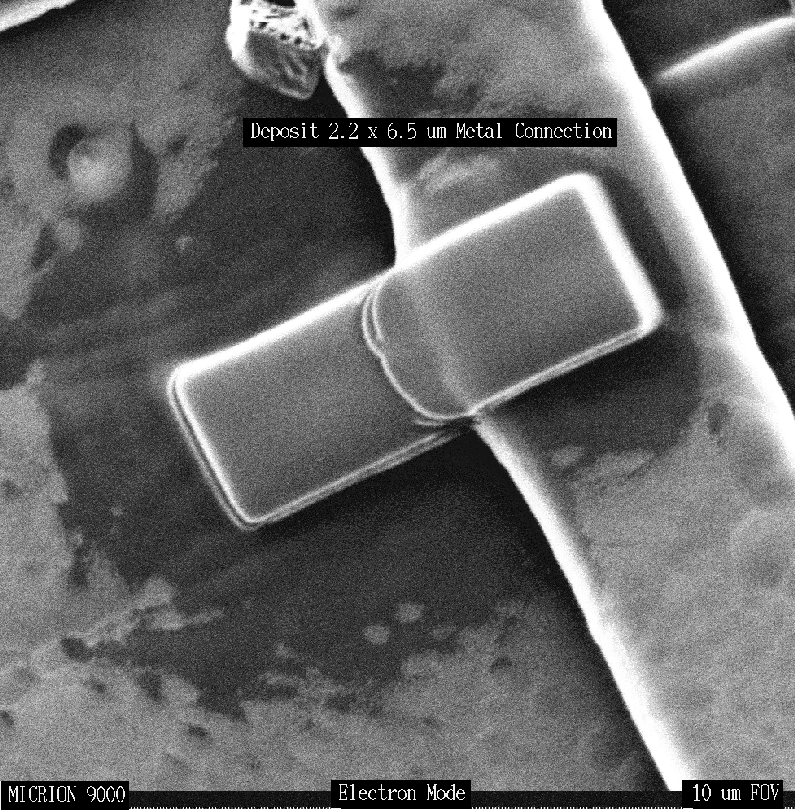
Photo 5 - Deposit the strap to make connection.
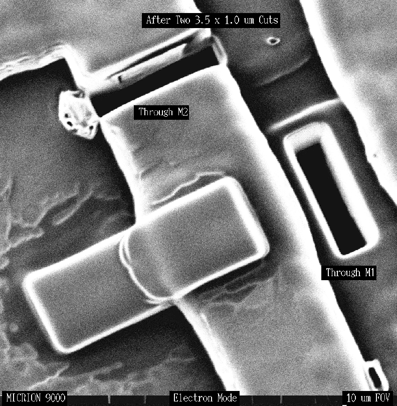
Photo 6 - Make isolating cuts (if necessary).
FIB cut and/or paste is performed when it is desirable to remove and/or deposit material (on the order of cubic micrometers) locally on an IC. If the IC being modified by FIB cut and/or paste is being analyzed for the cause of electrical failure, it should be thoroughly tested electrically prior to making the FIB modifications.
FIB cuts can be used to expose underlying conductors for electrical or electron-beam probing or other analysis, such as light emission microscopy. FIB cuts are also used to isolate or connect conductor lines. A combination of FIB cutting and pasting can be used to reroute the conductors in an IC. This can be useful in IC failure analysis to "patch" around a defective area; the part can then be retested to determine if a given defect was the cause of the observed failure. FIB cut and/or paste can also be used to test out ideas for simple design changes prior to going into production and for depositing bond pads for probing lines locally.
