System Maintenance occurs every Friday.
The concept of using a film with a temperature dependent fluorescence quantum yield to generate high resolution thermal maps of integrated circuits was first published in 1982 by Paul Kolodner and J. Anthony Tyson at Bell Laboratories [4]. Their first work described a technique which could yield thermal images with a thermal resolution of 0.006°C and a spatial resolution which was equipment limited to 15 mm. They noted that spatial resolutions of better than 1 mm were achievable with different optics and a better camera. This improvement in spatial resolution was demonstrated less than a year later in the second work published by the same authors [5]. The goal of this second work was to demonstrate the spatial resolution capability of the technique, which they measured to be 0.7 mm.
In the following years, a company called Lassen Research was licensed by Bell Laboratories to market turn-key fluorescent microthermography systems based on the work of Kolodner and Tyson. To the author's knowledge, only a handful of systems were sold, all within the AT&T system. This author's experience with FMI is with one of these systems and with subsequent development of a system to exploit this technology to its limit.
Word of the usefulness of FMI has spread throughout the failure analysis field, and now at least a half-dozen failure analysis engineers are developing systems on their own for their companies. The recent interest in FMI has caught the manufacturer of the fluorescing film, Eastman Kodak, by surprise. Since the compound of choice has not been used widely, the supply at the manufacturer was small. The renewed interest in the technique will hopefully be enough that supply problems do not deter interested engineers from using FMI in their laboratories.
During the late 1950s and early 1960s, scientists concentrated on a great deal of laser research. Some of this work dealt with the use of rare earth chelates as sources for use in liquid lasers. Rare earth chelates were identified as possible sources because of their well known fluorescence responses to UV or near-UV excitation sources. One of these compounds, EuTTA (europium thenoyltrifluoroacteonate) is the focal point for the fluorescent microthermal technique. The availability of compounds such as EuTTA is the main reason that the fundamental limitation on spatial resolution encountered in IR thermal systems could be overcome.
EuTTA is not the only compound available for FMI. In fact, there are chelates of all of the rare earth elements which include La, Sm, Eu, Gd, Tb, Dy, Tm, Yb, and Lu. The europium system was ultimately selected by the developers of FMI as the most suitable because of its temperature characteristics, emission/absorption characteristics, availability, and other qualities. Several other europium compounds might be suitable for FMI. Other b-diketone chelates of europium are available such as europium benzoylacetonate, europium dibenzoylmethide, and europium hexfluoroacetonate in addition to EuTTA. EuTTA, however, has the best fit for temperature dependent fluorescence quantum yield in the temperature range near room temperature.
To better understand the theory behind FMI, we need to discuss the process which gives the fluorescing film a temperature dependent fluorescence quantum yield. Fig. 4 shows the molar excitation coefficient (or, loosely, the absorption spectra) versus wavelength for EuTTA. These were measured for EuTTA in an ethanol solution. While FMI requires that EuTTA be suspended in a solid matrix, the data in Fig. 4 indicates the excitation wavelengths of interest. First, there is a broad absorption peak centered on 335 nm. This is where the TTA ligand absorbs energy. After about 360 nm, the amount of incident radiation that is absorbed falls off strongly. The two peaks at 460 nm and 525 nm are consistent with Eu3+ levels and are not of interest from an excitation viewpoint. The lack of absorption for wavelengths above 500 nm is significant, however, because it allows for a strong separation between the excitation source and the fluorescence emission.
Ultraviolet radiation excites the EuTTA fluorescence through an intermolecular energy transfer. The TTA ligand absorbs the UV light and then transfers the energy to the europium ion. While several fluorescence lines are excited, the transition from the Eu3+ 5D0 energy level to the 7F2 level is the most efficient. This transition generates the bright fluorescence line at 612 nm, which is used for FMI. Fig. 5 shows the emission spectrum for crystalline EuTTA at 25°C.
![Absorption spectra for EuTTA (in solution) [15].](/reference-material/failure-and-yield-analysis/failure-analysis-die-level/images/fluorescent-microthermographic-imaging-image-1-medium-2x.png)
![Absorption spectra for EuTTA (in solution) [15].](/reference-material/failure-and-yield-analysis/failure-analysis-die-level/images/fluorescent-microthermographic-imaging-image-1-small-2x.png)
![Emission spectra of EuTTA (Crystalline) at 25 °C [15].](/reference-material/failure-and-yield-analysis/failure-analysis-die-level/images/fluorescent-microthermographic-imaging-image-2-medium-2x.png)
![Emission spectra of EuTTA (Crystalline) at 25 °C [15].](/reference-material/failure-and-yield-analysis/failure-analysis-die-level/images/fluorescent-microthermographic-imaging-image-2-small-2x.png)
For thermal imaging applications, we need to know how the emission spectra of the compound changes with temperature. The temperature dependence of this europium chelate was considered a problem for liquid laser applications, but it is what FMI relies upon for image formation. Fig. 6 shows the measured absolute quantum yield versus temperature and Fig. 7 shows the decay time of the fluorescence yield versus temperature. Both of these plots were generated for EuTTA in an ether:isopentane:ethanol (5:5:2) solution. For the FMI application, a curve will need to be generated for each compound mixture that is used. These data have been included to illustrate the temperature dependence of EuTTA.
The fit curve in Fig. 6 was plotted using the equation
Q(T) = 0.398-0.07e0.031T
where Q(T) represents the quantum efficiency of the compound. The behavior of this compound over this broad temperature range is very predictable and provides a simple way to calculate the temperature of an object by imaging its change in quantum yield.
The information in Figs. 6 and 7 illustrates the intermolecular energy transfer between the TTA ligand and the europium ion. First, notice that the quantum efficiency falls off faster than the decay time with increasing temperature. This shows that we may have low quantum efficiency even at low temperatures due to a loss of excitation energy of the Eu3+ ion. The change in quantum efficiency with temperature is an indicator of the quenching of the whole system, while the fluorescence decay time is an indication of quenching of the fluorescence in the europium ion itself.
The standard application technique for using EuTTA for FMI is to incorporate the chelate into a PMMA (polymethylmethacrylate) matrix. A typical starting point is a solution consisting of 1.2 wt% EuTTA, 1.8 wt% PMMA, and 97 wt% MEK (methylethylketone). The MEK is a very high vapor pressure solvent that evaporates rapidly, leaving the EuTTA/PMMA mixture on the sample [4]. Typically, this mixture is spun on the sample and allowed to cure in an oven at 125 °C for about 30 minutes. Ideally, the film should only be several optical absorption lengths thick. At an excitation wavelength of 365 nm, a 300 nm film is approximately 3.5 optical absorption lengths thick. The idea is to have the film thick enough that most of the UV light is absorbed, but thin enough that the thermal profile of the sample surface is not distorted. As we will find out in later sections, the image processing required to create a thermal image reduces the influence of film non-uniformity on image quality. As such, the film should be as uniform as possible; however, taking great pains to achieve perfect uniformity of film composition and thickness is not necessary.
![Absolute quantum yield for EuTTA [16].](/reference-material/failure-and-yield-analysis/failure-analysis-die-level/images/fluorescent-microthermographic-imaging-image-3-medium-2x.png)
![Absolute quantum yield for EuTTA [16].](/reference-material/failure-and-yield-analysis/failure-analysis-die-level/images/fluorescent-microthermographic-imaging-image-3-small-2x.png)
![Fluorescence decay time for EuTTA [16].](/reference-material/failure-and-yield-analysis/failure-analysis-die-level/images/fluorescent-microthermographic-imaging-image-4-medium-2x.png)
![Fluorescence decay time for EuTTA [16].](/reference-material/failure-and-yield-analysis/failure-analysis-die-level/images/fluorescent-microthermographic-imaging-image-4-small-2x.png)
The EuTTA/PMMA composition can vary as needed for any specific application. Adjusting the EuTTA content will change the amount of fluorescent light emitted from the coated sample, and changing the amount of MEK in the mixture will thin the solution out for applications where spinning the sample is not practical. For instance, integrated circuits in packages are sometimes difficult to mount on a photoresist spinner. The use of a thinned out mixture would allow a thin film to be deposited without spinning the IC. Usually, spinning a packaged IC will cause the mixture to accumulate around the ball bonds, leaving a thick film in these areas. The thick film is not a problem unless the input structures are the areas of interest. For these applications, a thinner mixture or a higher spin rate would be in order.
One advantage of PMMA is that it can easily be removed once the thermal analysis is completed. Rinsing the sample in acetone will dissolve the film in several minutes. The use of other polymers such dPMMA, (perdeutero-poly-methylmethacrylate) will provide a stronger temperature dependence, but the additional cost of dPMMA is not justified. Other matrixes, such as Owens-Corning GR650 spin-on glass, have been successfully used, but make film removal more difficult.
Regardless of the film type used, accurate absolute temperature measurements are possible; but, because of the differences in the logarithmic slope of the quantum efficiency versus temperature curves for different materials, an accurate film calibration should be done for each type of premixed solution. The calibration curve can be easily obtained by using a hot/cold stage, a calibrated thermocouple, and the camera to be used for FMI. Simply record the total emission observed by the camera in a given time period with the sample at a given temperature. Varying the hot/cold stage temperature over as large a range as possible will give the best results. Samples such as blank wafers are ideal for this process since they will be close to the hot chuck temperature for the duration of the measurements. The emission versus temperature data can be plotted and a logarithmic slope can be found easily. Unless the composition of the mixture changes drastically, this measured slope need only be done once, especially if only relative temperature measurements are needed.
For higher temperature measurements, another europium compound, perdeutero-(tris-6,6,7,7,8,8,8-heptafluoro-2,2-dimethyl-3,5-octandionato) europium (dEuFOD) may be used up to about 200°C. dEuFOD has a much weaker temperature dependence both for fluorescence quantum yield and fluorescence lifetime than EuTTA [19].
A general consideration when working with rare earth elements is their inherent toxicity. The MSDS for EuTTA has been included in Appendix A for reference. Section IV of this MSDS lists the toxicity and health hazard data. Sections A and B indicate that the toxicological effects of this material have not yet been established. Always be sure to take proper precautions when handling EuTTA.
Now that we have an understanding of the fluorescent film properties which allow us to use this technique to generate thermal images, we need to cover how that information is converted to temperature data. Returning to Fig. 6, we recall that the quantum efficiency versus temperature can be represented as an exponential. Fitting an exponential function to the data in Fig. 6 gives us
Q(T)=0.398-0.07e0.031T
as the quantum efficiency versus temperature relationship. The light intensity at a given point, (x,y), on the image can be represented by
S(x,y)=I(x,y)·?(x,y)·r(x,y)·Q(T(x,y))
where I(x,y) is the illumination intensity, ?(x,y) is the optical collection efficiency, r(x,y) is the sample reflectivity, and Q(T(x,y)) is the quantum efficiency. In order to remove all spatial artifacts included in the I, ?, and r terms, and leave an image containing only thermal information, we can divide an image taken with the sample under bias (a hot image), by one without bias (a cold image). The result is a map of the ratio of quantum efficiencies between hot and cold images:


If we were working with a pure exponential, this ratio would be directly proportional to the difference in temperature, TH-TC. The problem with doing this directly is the 0.398 constant in the fit for Q(T) given above.
One way around this problem is to create a carefully measured calibration curve for a given film mixture using a given illumination intensity on a given optical setup, etc. and use that curve as Q(T) above. This method allows accurate absolute temperature measurements to be made, but adds a great deal of difficulty to the FMI process. Problems with this process arise from small changes in equipment that create changes in light collection from a sample at a given temperature. For example, since the fluorescence intensity decreases as the film gets hotter and the film degrades under exposure to UV light, the sample will appear hotter after repeated imaging sequences. The degradation will require repeated removal and re-application of the film for accurate results.
In most applications, relative rather than absolute temperature measurements are needed; therefore, the image math can be simplified greatly with only a slight loss in accuracy. We need to stress that the slight accuracy change does not decrease the sensitivity of the technique or the smallest change in temperature that can be resolved.
To modify the process and allow for relative temperature changes, continue with the equation for the ratio of quantum efficiencies that we had before, take the natural logarithm, and plot the result for temperatures around room temperature. This gives us,


This equation is plotted in Fig. 8 with the cold temperature, TC, set at 28 °C.


The linear fit in Fig. 8 can be represented by the following equation:


The standard deviation in the slope is 0.0006909, or less than one percent. The slope of the linear fit is what we need for temperature conversion. Once we have the slope, the rest is easy. Simply divide the natural log of the quantum efficiency relation by the slope. The result is the relative temperature change of a given pixel location.


By taking the natural log of the ratio of the light intensities from a hot and cold image, we can divide the result by a constant and have a relative temperature measurement. This is the method presented in the literature [4,5] for use in FMI.
The examples that have been used here are based on the quantum efficiency versus temperature from EuTTA in solution, as described in the previous section. For EuTTA combined in a polymer or glass matrix, the fluorescence quantum efficiency will have the same temperature dependence as the previous equation, as this is dictated by the intermolecular energy transfer process. However, the end values will be different. Published values for the slope of the linear fit in Fig. 8 for EuTTA in a dPMMA matrix are approximately -0.047 /°C [5]. This number will be different for EuTTA in PMMA or GR650 glass, as well as for EuFOD in dPMMA. Whatever chemistry is chosen, a calibration curve as outlined above must be made.
As an example, if a camera with 16-bit grayscale resolution is used and we assume a published value of the logarithmic slope of -0.047 /°C, the best possible thermal resolution would be:


Compare the equation above with an 8-bit gray scale camera:


This result will be referred to in the next section, which discusses hardware requirements.
Standard techniques can be used to reduce noise in the resulting thermal image. Image averaging on both the hot and cold images can be done prior to processing. Various techniques can be used after processing to enhance the thermal artifacts.
Essentially, three main system components are required for FMI. These components include a light source, a camera system, and an optical platform. This section discusses these areas and indicates the differences between each possible choice.
The light source used for fluorescence excitation has the most possible choices. The absorption spectrum for EuTTA (Fig. 4) indicates that we are interested in ultraviolet sources in the approximate range of 210 nm to 365 nm. Sources with wavelengths greater than 365 nm will require higher intensities to excite the fluorescence, and thus are impractical. UV sources always present a hazard to the human eye, so the use of proper eye protection is mandatory.
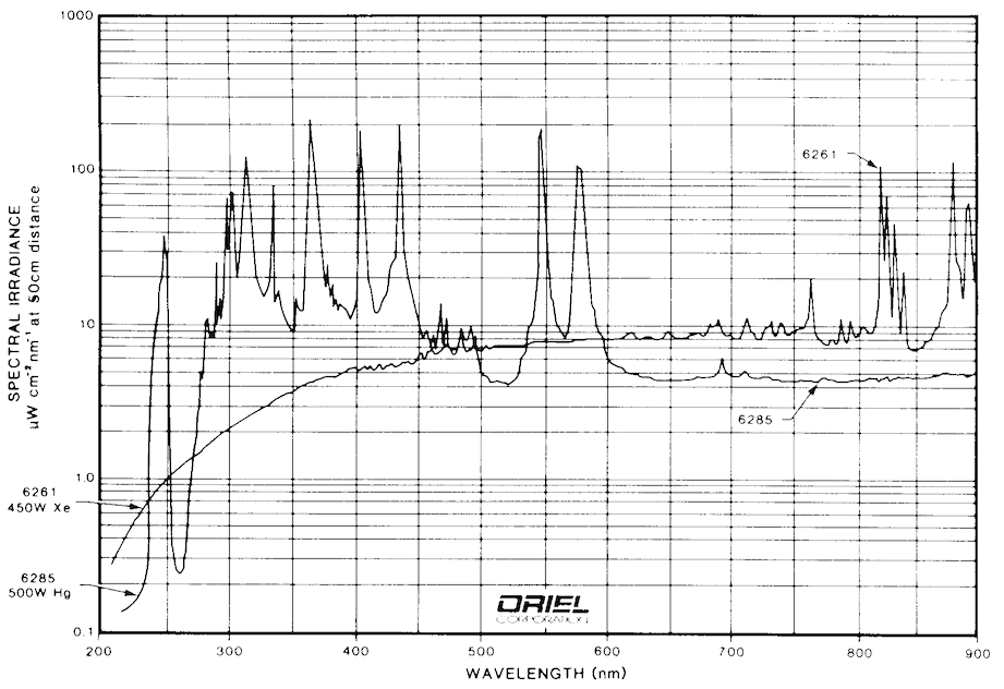
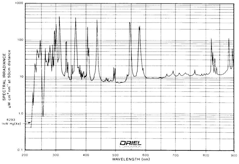
Most of the FMI systems currently in operation use arc lamps as their excitation sources. The most common lamps for UV applications are mercury, xenon, and mercury/xenon types. Examples of spectra for these types of arc lamps are shown in Fig. 9 and Fig. 10. It is clear from these figures that any of the three types of lamps suit the application well. Mercury bulbs have well-known spectral peaks in the UV range and several that extend into the visible range. Xenon lamps have peaks in the upper end of the visible range, but have a broad continuum of output that extends usefully into the UV. Mercury/Xenon lamps combine the two spectra to create a broad range general purpose light source.
Arc lamps have been manufactured for many years. As such, one may be in storage somewhere in an old laboratory. While this old lamp may be good for demonstrating the FMI technique, modern arc lamps have benefited from years of research and are more stable sources. Stability of the light source, as evident from the last section, is one of the limiting factors in creating high temperature resolution images. If you decide to use an arc lamp as an excitation source, inquire about the stability of the light output as a key factor toward deciding which unit to purchase.
The other obvious choice for excitation source is a laser. Lasers differ from arc lamps in that all of their optical energy is in one narrow wavelength band rather than being spread over a continuum. Since all of the light output is within the wavelength range of interest, lasers are also more efficient. Table 3 lists some of the different laser systems and their respective lines. About half of the systems are listed as CW, or continuous wave, systems. These lasers have a continuous light emission. The remaining systems are pulsed, meaning they cannot sustain continuous emission and emit light in short pulses, usually with repetition rates up to several kilohertz. The choice between laser systems is usually cost. Many of the CW systems listed are very large laser systems, such as Argon Ion lasers, that have a weak line suitable for FMI. The problem is that you may have to purchase a laser with an output of several watts to yield several milliwatts for the UV line you need.
| Wavelength (nm) | Laser System | Pulsed or CW |
|---|---|---|
| 190-1000+ | Dye | pulsed |
| 220-390 | Frequency doubled die | CW |
| 325 | HeCd | CW |
| 330-380 | Neon | CW |
| 333-364 | Argon Ion | CW |
| 333.6 | Argon | CW |
| 337 | Nitrogen | pulsed |
| 345-500 | Ti:Sapphire | pulsed |
| 351 | XeFl | pulsed |
| 351.1 | Argon | CW |
| 351 or 355 | Nd:glass | pulsed |
| 365 | Nd:YAG | pulsed |
Pulsed systems, such as the dye lasers or solid state lasers, can be relatively inexpensive, but for FMI, two successive exposures (one for the cold image and one for the hot image) may contain different numbers of pulses from the laser. Although this may sound like a small problem, it adds another process that may reduce the temperature resolution of the system. Dye lasers do have the ability to be tuned over a broad range of wavelengths, giving them an advantage when and if other fluorescent compounds are developed. For the system being developed at Sandia, a 15 mW HeCd laser system has been chosen because it is a small CW system that is relatively inexpensive. Other known systems use Hg arc lamps or pulsed dye lasers.
The next step for system design is to choose a camera system. Existing systems, without exception, use slow-scan CCD cameras. In this case, slow-scan refers to the frame rate at which data is read out of the CCD array. Television cameras adhere to the NTSC video standard where the CCD array in a CCD camera would be read at a rate of 30 frames per second. While this frame rate is good for television cameras, it is relatively poor for quantitative analysis of the image content. High quality TV cameras can approach 400 lines of information in about 500 fields with about 8-bits of dynamic range.
As we saw in the previous section, using a camera system with 8-bits of dynamic range would limit system sensitivity to roughly 0.4% change in quantum efficiency, or 1 part in 256. Slow-scan cameras are available with 12 to 16-bits of dynamic range and can thus image changes in intensity from 1 part in 4096 to 1 part in 65536 in an image of size ranging from 512 by 512 to 1024 by 1024 pixels. This translates into an order of magnitude gain in possible difference in temperature resolution.
Slow-scan cameras, since they do not adhere to TV standards, are designed to stare at a field of view and integrate for a variable length of time. For a situation where a very small amount of light is being emitted, the camera can stare at the field of view for several minutes to several hours, or until the detector becomes saturated. In contrast, when using TV cameras for low light situations, it is necessary to grab and add video frames together, which also adds noise. Image averaging can be used to help remove noise, but it doesn't boost signal.
Noise in collected images is a second factor that will limit temperature resolution. Slow-scan cameras are almost always either peltier or liquid nitrogen cooled. Cooling helps to eliminate thermal generation of electron-hole pairs, which can fill up CCD charge wells with noise instead of image signal. Peltier or liquid/peltier cooled systems generally operate at -39 °C or so and, as a result, generate only several electrons per second of noise with a well capacity of several hundred thousand electrons. Liquid nitrogen cooled systems, by cooling to a much lower temperature, keep the noise down to several electrons for every ten to one hundred seconds. With these systems, the readout electronics also add a small, but predictable amount of noise to the image, typically several electrons or tens of electrons per pixel. The noise qualities of these cameras and their integration capabilities, along with spectral sensitivities past 1 micron, have prompted manufacturers of light emission systems to use them in lieu of TV cameras.
In general, virtually any camera which can yield an image in digital format, either directly or by frame grabbing, can be used for FMI. While TV cameras will work, they may become the limiting factor for thermal resolution. In applications where the technique is needed, but funds to build a system are scarce, TV cameras may be a good solution. However, the use of slow-scan CCD cameras will insure that the camera is not the limiting factor in system performance.
Lastly, the optical platform to house the excitation source and camera must be decided upon. In order to electrically bias the sample, probe stations provide an obvious choice for an FMI system. Most systems used for probing fine geometries have optics boxes that have TV camera ports. The most common optics assemblies are made by Bausch & Lomb and Mitutoyo. Since they are used during probing, the lenses on these systems are extra-long working distance, but have to sacrifice some optical quality.
Standard metallographic microscopes generally have superior optical systems, but suffer from short working distance objectives and limited facilities for electrical biasing of the sample. Most microscopes do have c-mount camera ports or other ways of attaching a camera.
Depending on whether the application falls into the category of primarily packaged ICs or wafer level analysis, the optical platform that best suits the most frequent use of the system should be used.
Once the three main system components have been selected, the remaining considerations are relatively small. A computer with image processing capabilities that can handle the requirements outlined in the previous section is needed. The number of possibilities for this part of the system is too great to warrant much further discussion. It is sufficient to state that virtually any computer that you can get the image to will work without affecting performance, other than image processing speed, of course.
Traditional FMI systems input the excitation source through a UV grade fiber optic cable onto the sample at an oblique angle [4]. This does remove many headaches from the optical system, but tends to limit the amount of light that can be easily sent to the sample, especially when using high magnification, shorter working distance lenses. Even on a probe station, a 50x lens will have a short enough working distance to complicate sample illumination. The use of a "through-the-lens" type of illumination removes the problems of sample illumination, but adds the problems encountered with non-UV transparent optics found in most microscopes. Generally, standard optical components offer transparency for light with wavelengths greater than about 370 nm. UV grade components are available because of the market for people doing fluorescence work, but the components, such as lenses, tend to be very limited in application and type, (e.g. magnification, working distance, numerical aperture, etc.).
The final system component needed is a custom interference filter to filter out all of the fluorescence except the dominant line at 612 nm as shown in Fig. 5. Most manufacturers of optics or filters will be able to put together a filter sandwich that can meet the requirements of FMI. A filter with a bandwidth of about 2 nm to 4 nm will be sufficient.
Now that we have discussed some of the system design considerations, it would be beneficial to describe some of the systems that have been assembled to do FMI.
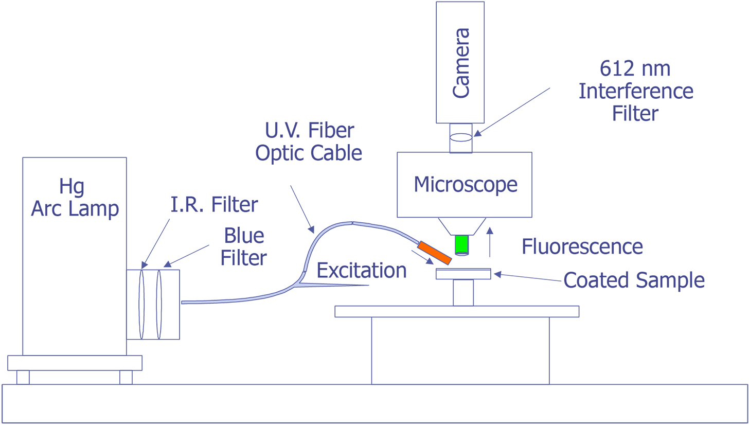
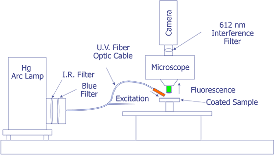
First, in their original work, Kolodner and Tyson [4,5] describe what they felt would be a typical system for FMI. They did not provide details about the optical system; however, they used a probe station and mounted the slow-scan CCD camera with the interference filter in front on the TV camera port. Their first CCD array was a 100 x 100 array, but they later upgraded to a camera with a 384 x 576 array that was peltier cooled. They sent the light from a 100 watt Hg arc lamp through IR and blue-glass filters and a fiber optic cable and brought it to focus on the sample at an oblique angle. Image processing (remember that this is circa 1983) was done on a PDP 11/73 type computer. This system worked well enough that they could measure 0.01 °C thermal and 0.7 mm spatial resolution. The only systems that were known to be commercially marketed to FMI were virtually identical to this system, but benefited from some computer improvements. A system configured in this manner is illustrated in Fig. 11.
The system under development at Sandia represents a good contrast from the system just described. Sandia decided to implement the system on a Zeiss LSM (Laser Scan Microscope) and to illuminate the sample through the lenses using a 15 mW HeCd laser. The laser will be pumped through a UV grade fiber optic cable and UV transparent objectives. This arrangement is illustrated in Fig. 12. The bulk of the problems that are being encountered at the time of this writing occur because the optics are virtually opaque to light at 325 nm. Nevertheless, possibly useful UV objectives are available from a third party, and the manufacturer of the microscope has ideas on how to pump the light to the objectives. Aside from this problem, system implementation is straightforward.


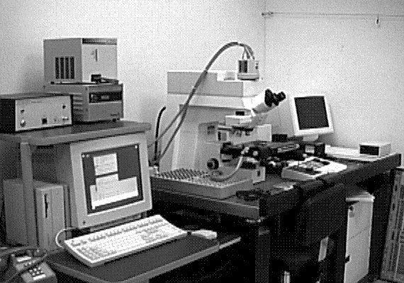
The Photometrics slow-scan CCD camera chosen features a liquid/peltier cooling system interfaced into a Sun workstation through a remote VME bus. The CCD array chosen was a Tektronics TK512 device with 512 by 512 pixels and charge wells averaging over 600,000 electrons. The deep wells allowed us to use the full 16-bit dynamic range available as an option on the camera electronics. The array was also thinned and was back illuminated to enhance the light collection efficiency. Larger arrays, such as the of 1024 x 1024 or 2048 x 2048 types were available, but they added significant cost and reduced the cell dimensions and the full well capacity. Figure 13 (in the photograph section) shows the LSM with the Photometrics CCD camera mounted, the Sun workstation used to control both the microscope and the CCD camera, and the HeCd laser, barely visible, to the right of the microscope. When complete, the microscope will be contained in a light-tight, interlocked box, both for the exclusion of stray light and for safety reasons.
The Sun computer platform was chosen so that the collected images could be directly imported into Khoros, an image processing software package written by the Khoros Group in conjunction with the University of New Mexico [21]. Khoros has many more capabilities than FMI requires, but its power for this application comes from being able to control both the LSM and the CCD camera directly through easy-to-make Khoros routines called glyphs. Once the control glyphs have been established, a single mouse click can take the series of images and process them into a thermal profile.
This tutorial will lead readers through the theory behind the technique, describe the hardware and image processing requirements needed, and discuss some example applications. The preceding sections on blackbody radiation and IR thermography were included so that readers can understand thermal imaging concepts, the nature of the signals that are present, and the reason for the fundamental limitation on spatial resolution imposed by imaging IR radiation. While IR thermography is invaluable to the microelectronics industry, its applications are limited when the areas of interest are sometimes an order of magnitude smaller then the available spatial resolution. FMI is unchallenged in applications such as these.
FMI is performed in a similar manner to liquid crystal with two main differences. The two main differences to keep in mind are (1) the application of the fluorescing compound, and (2) the image acquisition.
The fluorescing compound (in this text EuTTA) is applied by making a 1.2% EuTTA, 1.8% polymethylmethacrylate, 97% methylethylketone mixture. After mixing up the solution, apply a small amount of the solution to the die surface using a dropper. Spin the sample on a grinding wheel to make the solution cover the entire die. The solution may be rather thick at the bondpad because of the surface tension of the bond wires. This is not a problem unless you need to examine circuitry directly adjacent to the bond wires. In this case, spin the sample at a faster rate to reduce the accumulation at the bond wires. Bake the sample in an oven at 125°C for 30 minutes to evaporate the methylethylketone and cure the sample.
Next, place the sample under a scanning optical microscope and start the software that controls your CCD camera. Be sure to direct the UV light away from the sample as much as possible because the light will bleach the EuTTA film, making your measurements less sensitive. First, take an image of the IC in a cold "off" condition. Do this by getting your software ready to capture an image. When you are ready, turn on the UV source and capture the image. Immediately after you are done capturing the image, turn the UV source off. Power up the IC in the high current condition, turn on the UV source and use the software to capture an image. Once again, immediately after the image is acquired, turn off the UV source. You should now have a hot image and a cold (background) image.
Use your software imaging package to perform a division of the hot image from the background image. This will leave you with an FMI image showing the hot spot. It may be necessary to performing averaging to increase the sensitivity of the technique.
After you are through performing FMI, you can rinse the material off the die using acetone. Rinse the sample in acetone for several minutes. The acetone-EuTTA-PMMA mixture is toxic and should be handled and disposed of with this in mind.
FMI is not a destructive technique and can be performed on the IC once the IC is delidded. Because the technique tends to be more involved than light emission or liquid crystal, you would typically perform this technique after both of these techniques. After you have performed FMI, you can remove the EuTTA/PMMA material by rinsing the sample with acetone for several minutes.
