System Maintenance occurs every Friday.
Electron Beam Induced Current (EBIC) is a scanning electron microscopy (SEM) imaging mode that localizes regions of Fermi level transition. EBIC is primarily used to localize buried diffusions and semiconductor defects. Minority carrier diffusion lengths and lifetimes have also been measured using EBIC, but these measurements very rarely apply to failure analysis. EBIC images are produced by monitoring the nonrandom recombination current of the electron-hole-pairs generated when an electron beam is scanned across a semiconductor. The recombination current may be increased or decreased by biasing the IC. Additional testing information can be useful in selecting the optimum conditions for performing EBIC.
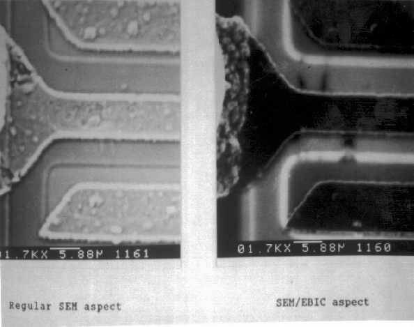
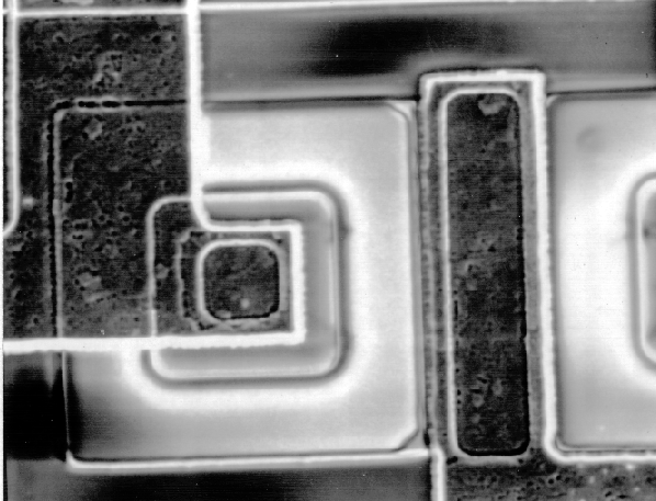
When conventional optical microscopy is either difficult or impossible to implement for junction localization, EBIC imaging is performed to localize diffusions (such as diode or transistor junctions), particularly those buried below passivation or metal conductors. When the energy of the primary electron beam is increased so that electron-hole-pairs are produced near junctions under examination, recombination current in buried diffusions produces an EBIC image.
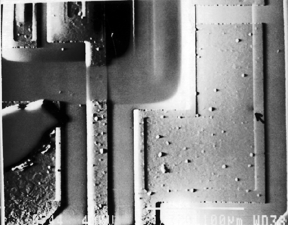
EBIC imaging is also useful in localizing semiconductor and junction defects, such as stacking faults, dislocations, EOS/ESD damage, diffusion spikes, and diffusion pipes. These defects produce local variations in the Fermi levels or built-in potentials that can enhance or diminish the recombination current and hence the EBIC signal.
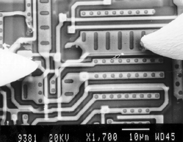
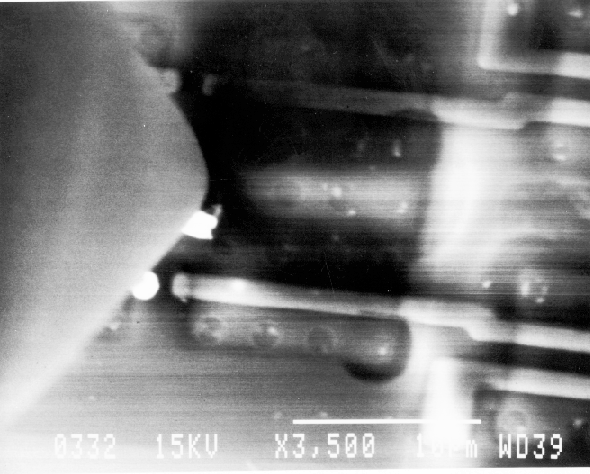
While the EBIC technique can be useful in localizing diffusions and semiconductor defects three factors limit EBIC's effectiveness. First, EBIC can only observe recombination currents relative to the test nodes selected. When the IC's power leads are used as test nodes and no charge flow occurs relative to the power pins, a large recombination current across a p-n junction connected to the IC's power leads through a complicated feedback network will not produce an EBIC signal. Properly selecting which IC leads to use as test nodes, biasing the IC (and thereby "turning on" current paths to the IC's leads), and using small mechanical probes to access conductors connected directly to the junction(s) of interest increases the observability of recombination currents deep inside the IC logic. The ground and power leads of an IC are normally the initial test node choice for EBIC imaging of structures deep inside the IC because of their "global" nature, but other leads may be used if the IC's design or electrical testing suggest a better combination.
Secondly, EBIC will produce irradiation damage on MOS devices. Bipolar structures are relatively immune to the electron beam's ionizing radiation, but the primary electron beam energies required to generate EBIC signals will immediately damage MOS gate oxides. This damage occurs in the form of fixed oxide charge and interface trap creation/occupation. Consequently, the threshold voltage of MOS transistors can be changed by volts, thereby dramatically altering IC performance. The damage can normally be annealed by a 120°C bake for ~4 hours. Thirdly, even if no access or damage limitations occur, the EBIC signal will normally include recombination current information from a majority of the diffusions on the IC using power and ground as test nodes. This additional information can make it difficult to identify the site of a particular anomaly. Using light emission, liquid crystals, or another failure analysis technique to reduce the area for EBIC examination will reduce the amount of extra EBIC information and increase the likelihood of locating an EBIC defect.
To obtain EBIC information, increase the primary electron beam energy until the interaction volume intersects the region to be examined. When the primary electron beam is scanned across an IC, collisions in the semiconductor will form electron-hole pairs within the bulk of the IC. The relatively low ionization energies (less than 10 eV) of the materials used in IC manufacturing allow a single 10 keV primary electron to produce as many as 500 to 1000 free electron-hole pairs. These pairs usually recombine randomly in the material; however, if production occurs in a space-charge (depletion) region, the charge carriers will be separated by the junction potential before recombination producing an EBIC current. The large number of pairs per primary electron generates an EBIC signal much larger than the incident beam current. Using an amplification configuration as shown in Figure 1, the recombination currents can be amplified and displayed on the SEM.


Usually the power and ground inputs are used as test nodes because of their global nature across the IC; however, other node combinations may be used if indicated by the failure history. In contrast to secondary electron and backscattered electron imaging, the EBIC signal detector is the IC itself. By controlling the primary electron beam energy, the depth of the recombination current source as well as its X-Y distribution can be determined.
Since EBIC requires interaction between the primary electron beam and the junctions or defects of interest, optically opaque layers may be "probed through" by increasing the primary electron beam energy. The following expression can be used for a rough estimate of the primary beam energy required to reach a given structure:
R=0.022 E1.65
where R is the distance below the surface and E is the primary electron beam energy.
For test structures with no gate oxide or oxide capacitors, such as a bipolar IC, no irradiation damage will occur. Thus, starting with a very high primary electron beam energy is possible. This will insure that the primary electron interaction volume reaches the buried conductor and will also reduce surface passivation charging by "shorting" the substrate to the surface through the interaction volume.
EBIC is performed to locate diffusions or defects. For MOS ICs, EBIC should be performed after the application of other, more benign failure analysis techniques. EBIC does have the advantage of being able to probe through passivation and metal layers, so if a junction location is desired or a defect is indicated by other test methods, EBIC can be applied before layer removal. Bipolar ICs are relatively immune to the irradiation of the SEM's electron beam, and EBIC can be used without the problems of MOS irradiation sensitivity. Because no MOS structures can be damaged by primary beam irradiation, high energies can be used to insure that the interaction volume reaches the structures of interest. The higher energies will also reduce surface charging by "shorting" the surface passivation to the substrate. While surface layer removal can make it easier to reach buried regions at lower primary electron beam energies, the possibility of failure site alteration during deprocessing still exists. EBIC can eliminate or reduce the need for surface layer removal during failure site localization.
Controlling the primary electron beam energy and monitoring the EBIC signal strength can provide semi-quantitative depths of the structures being examined. However, variations in beam energy, IC material densities, and beam currents make accurate depth measurement difficult.


