System Maintenance occurs every Friday.
System Maintenance occurs every Friday.
Electron beam probing is a special case of voltage contrast imaging where the operation or electrical function is displayed as a video or computer image. As the name implies, voltage contrast imaging is performed during dynamic rather than static operation of the component(s). This mode of operation requires that a connection be made to the circuit via feedthroughs in the SEM vacuum chamber and that electrical bias be applied. The complexity of the component and node coverage desired determines the number of pins and cables required. If it is possible to isolate the suspected area of root cause of failure, the vector set need not be large. However, isolation is not always possible; and, in such cases, we have used automated test equipment (ATE) such as a Sentry or Advantest tester to apply the full test vector set. No special detector is required to achieve voltage contrast on semiconductors with a voltage swing of about 1 volt while being operated at low to moderate frequencies. To avoid radiation damage to CMOS circuits, it is recommended to use an accelerating voltage of about 1 kV. (The low energy of the electron beam in the range of 0.8 to 1.2 keV is usually sufficient to avoid radiation damage to MOS devices.) For circuits not sensitive to electron beam radiation, using an accelerating voltage up to 30 kV may be possible. With non-sensitive components, experiment with the accelerating voltage to determine which setting gives the maximum contrast. Other parameters that can be altered or adjusted to obtain more contrast include: the column aperture, the beam sweep rate, and the component bias voltages.
The e-beam prober was designed to improve the diagnosis and characterization of complex integrated circuits. The Schlumberger IDS-5000, for example, has integrated CAD/CAE software and tools that allow design, reliability, and failure analysis engineers to work together and share information. An automated prober can be succinctly described as the marriage of an SEM column and vacuum chamber with an engineering workstation. The equipment uses the dynamic voltage contrast imaging principle and generates real-time images that can be used to characterize and monitor voltages of specified areas.
Waveforms are produced by raster scanning a beam of primary electrons (beam energy ~ 1 keV) across the surface of the circuit. The primary electrons interact with the electrons on the surface of the component and through this electron/electron interaction, secondary electrons are produced and emitted from the surface. A secondary electron detector is positioned near the circuit to collect the emitted electrons and the rate of collection depends on the surface potential of the IC. The SEM column varies its internal bias to maintain a constant collection rate. This bias produces the displayed waveform. Commercial test systems result from the increased needs in fault diagnosis in advanced ICs and the improvements in electron-beam equipment used in basic and applied research. The spatial resolution of commercial probers is less than 0.5 micron with a claimed maximum acquisition frequency of 5 GHz.
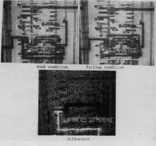
DFI is a technique for acquiring and imaging faults in random logic devices. Logic states for both faulty and fault free devices are imaged separately by means of stroboscopic voltage contrast in a scanning electron microscope or e-beam prober and are then stored as incremental time sequences of images. These sequences represent the time evolution of states during a particular device test and are then compared in an image array processor. The divergences or changes between the faulty and the fault-free device evolutions represent faults, which are then displayed on a screen. The technique applies to the solution of failure analysis problems.
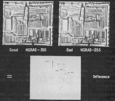
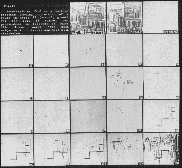
Figure 3 conceptually represents Dynamic Fault Imaging. The device of interest is operated in the scanning electron microscope with stimulus applied from a tester or pattern generator. The voltage contrast video is acquired stroboscopically by looping on a small portion of the vector set and acquiring a voltage contrast image of the device. This process is repeated for the number of frames (or vector states) desired. The entire process is repeated again for a reference device. Each pair of images (one from the device of interest and one from the reference device) is digitally subtracted, leaving only the differences (see Figure 4). This allows one to image the progression of malfunctioning logic with respect to time (see Figure 5). More importantly, for failure analysis, the failure at the device pins can be traced backward to the initial malfunctioning node. The analyst then has a good location in which to start looking for the defect.
This technique is primarily used to inspect metal and polysilicon interconnections, but it can also reveal information regarding diffusions in regions where the interconnects are unobstructed. Using the acquired images, inspections trace the electrical signal path or circuit functionality.
A beam of low energy primary electrons (~1 keV) is raster scanned across an area of interest on the IC, and the rate of secondary electron emission is proportional to the local surface potential. The test engineer collects the image while the component is under bias and in dynamic operation. This technique permits a non-destructive method of testing both passivated and non-passivated ICs.
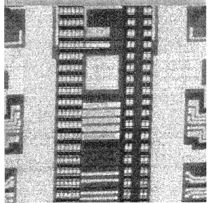
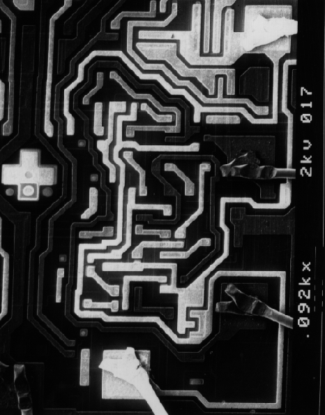
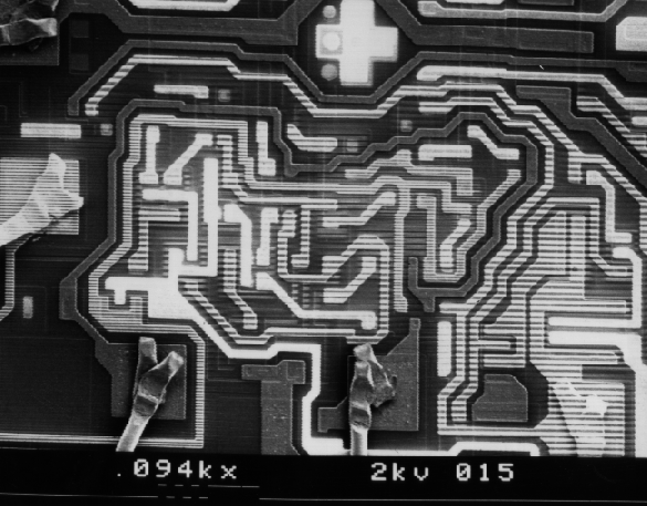
Electron Beam Probing can be applied on both single and multilayer interconnect devices with the passivation intact. Those new to dynamic voltage contrast should use components that are passivated when working with complex circuits; otherwise, the images acquired will denote all the interconnects with either a dark or bright contrast. When a component is passivated, only those interconnects that are changing potential are shown with either a dark or light contrast, simplifying the analysis considerably (see capacitively coupled voltage contrast for more details). All constant voltages are seen as a uniform gray. When examining a non-passivated complex IC, it may be necessary to use an image processor to digitally enhance the data. For example, subtraction of images uses the same image processing equipment set as that used during dynamic fault imaging, DFI. One advantage of using a non-passivated component would be the ability to observe the "barber pole" and its connectivity and routing. Figure 1 shows a secondary image of an unpassivated IC under static operating conditions. Figure 2 shows the same IC under dynamic operation and the resulting "barber poles."
Here are some "rules of thumb" to apply that can avoid cross talk errors if the line width is equal to the spacing:
(1) Quantitative analysis of waveforms should be possible if the interconnect line width is at least four times the passivation thickness.
(2) Logic state analysis should be possible if the line width is greater than the passivation thickness.
(3) Errors due to stray electric fields of neighboring lines become dominant at small line geometries.
For a 2-level metal technology where the bottom level is being probed and neighboring lines on the upper level are present, the limitations are:
(1) Quantitative waveform measurement may not be possible for line geometries used in VLSI technologies.
(2) Logic state analysis is limited to line widths equal to line spacings greater than 3 to 5 microns, depending on the passivation thickness.
Some examples of the aforementioned defects are shown below. Figure 6 shows a dynamic voltage contrast image of metal interconnect open at a polysilicon step.
An example of the use of dynamic voltage contrast imaging is now given to illustrate how analysis time on a VLSI IC can be decrease or minimized. The details of this example were taken from the analysis of a 256K E2PROM that failed electrical testing after the completion of a high temperature (250°C) memory retention test.
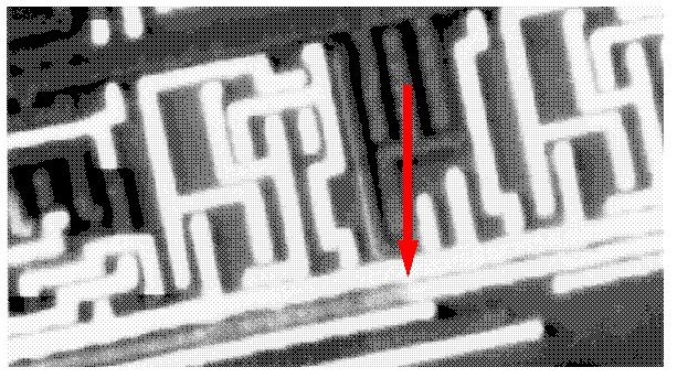
The electrical data obtained from an ATE indicated that the component was failing several memory addresses. From optical inspections, the analyst could identify 64 columns of 8 bits each and 512 rows of memory cells. Correlating the failing addresses to the memory architecture, the failure mode suggested the existence of a "bad" column. After putting the part into the SEM chamber and making the appropriate electrical connections, failing addresses of the column were selected and the memory chip was repeatedly write/read cycled. The selected column was obvious since it had a different contrast when compared to non-selected columns. By scanning the length of the selected column, the location of the defect became evident. Figure 7 shows the dynamic voltage contrast image of the defective bit line in the bad column. Figure 8 shows a higher magnification of the failure site. The electrical potential discontinuity is markedly displayed as an abrupt contrast change in the defective bit line. If the bit line were functioning properly, it would have a uniform contrast as the others in the column are shown. To complete the analysis, analysts used the manufacturer's data book information to determine that the defective bit line could indeed cause the failure signature of multiple failing addresses of the component. Voiding of the metal bit line during the high temperature anneal was determined to be the root cause of failure.
Since electron beam probing is a relatively benign technique, it can be performed immediately after package delidding/decapsulation if desired. However, since the amount of information in the voltage contrast image is enormous, it usually makes sense to try rapid localization techniques first. Techniques such as light emission, low energy CIVA, LIVA, TIVA, Liquid Crystal analysis, and Fluorescent Microthermal Imaging should be tried first to localize the defect. If these techniques are unsuccessful, then an approach such as electron beam probing should be tried.