System Maintenance occurs every Friday.
System Maintenance occurs every Friday.
Airbag sensors. Digital Light Processing™ projectors. Inkjet printers.
These examples are only a few of the applications for microelectromechanical systems (MEMS), which have quickly become one of the fastest-growing segments in the semiconductor industry. MEMS devices, also referred to as Microsystems Technology (MSTs) or Micromachines, promise to produce smaller, cheaper, more reliable systems--yet can the technology deliver on these promises?
Semitracks' latest 2-day MEMS Technology course focuses on the design, operation, packaging, reliability, and testing of MEMS devices, with an emphasis on packaging. The large surface area to volume ratio in MEMS devices creates unique challenges--for example, surface effects such as electrostatics and liquid wetting dominate volume effects such as inertia or thermal mass. Yet in spite of these poorly understood properties, MEMS retain the potential to revolutionize the electronics market.
$1,295
Add To Shopping Cart
Please note: If you or your company plan to pay by wire transfer, you will be charged a wire transfer fee of USD 45.00.
Please email the printable registration form for public courses to us at the email address on the form to complete your order.
If you have any questions concerning this course, please contact us at info@semitracks.com.
If a course is canceled, refunds are limited to course registration fees. Registration within 21 days of the course is subject to $100 surcharge.
The goal of the course is to give you a two-day overview of MEMS technologies by covering design, manufacturing, packaging, reliability, simulation, and testing. You'll gain an in-depth knowledge of challenges and opportunities associated with bringing MEMS and MST's to market through the course's focus on three key topics:
Our courses are dynamic. We use a combination of instruction by lecture, problem solving, and question/answer sessions to give you the tools you need to excel. From the very first moments of the seminar until the last sentence of the training, the driving instructional factor is application. The course notes offer hundreds of pages of reference material that the participants can apply during their daily activities.
Our instructors are internationally recognized experts. Our instructors have years of current and relevant experience in their fields. They're focused on answering your questions and teaching you what you need to know.
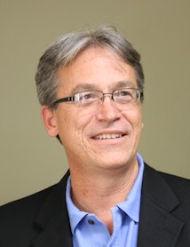
Steve Groothuis received a Bachelor's in Physics (1983) from Michigan State University and Masters in Physics (1991) from the University of Texas. He began work in the Central Packaging Group, Texas Instruments in Dallas in 1983 as a Group Member of the Technical Staff performing semiconductor package development, design, testing, and simulation. Prior to leaving TI, he managed the engineering staff in TI's Advanced Semiconductor Packaging Lab. In 1997, he was a Multiphysics Industry Specialist for ANSYS Inc. defining Computer-Aided Engineering simulation software market plans, strategic accounts management, Electronics Packaging, MEMS Device Simulation initiatives, and product development for the Electronics Industry. From 2000-2008, he was with Micron Technology in positions from Senior Package Engineer in the Assembly and Packaging Department to Technology CAD, and Analysis Manager in the Process RD Department at Micron Technology. His responsibilities included device and process simulations for new cell designs, supporting most aspects of semiconductor package simulations, and new technology assessments.
Currently, Mr. Groothuis is a Principal Consulting Engineer with SimuTech Group Inc. He is actively involved in developing and winning new business opportunities for Finite Element Analysis (FEA) and Computational Fluid Dynamics (CFD) consulting projects. His efforts are focused on vertical markets such as Microelectronics, Semiconductor Packaging, Wafer Fabrication, NEMS/MEMS, Nanotechnology, Solar Energy, Wind Energy, and Consumer Electronics.
He has published over 30 papers at various conferences in semiconductor packaging, reliability, and numerical analysis. Mr. Groothuis is a Senior Member of the IEEE and has participated in ASME and JEDEC standards committees.