System Maintenance occurs every Friday.

EOS, ESD and How to Differentiate

Electrical Overstress (EOS) and Electrostatic Discharge (ESD) account for most of the field failures observed in the electronics industry. Although EOS and ESD damage can at times look quite similar to each other, the source each and the solution can be quite different. Therefore, it is important to be able to distinguish between the two mechanisms. The semiconductor industry needs knowledgeable engineers and scientists to understand these issues. EOS, ESD and How to Differentiate is a 2-day course that offers detailed instruction on EOS, ESD and how to distinguish between them. This course is designed for every manager, engineer, and technician concerned with EOS, ESD, analyzing field returns, determining impact, and developing mitigation techniques.

Register for this Course

Cost

$1,295

Pay Via Credit Card

Add To Shopping Cart

Pay Via Purchase Order/Check

Please note: If you or your company plan to pay by wire transfer, you will be charged a wire transfer fee of USD 45.00.

Please email the printable registration form for public courses to us at the email address on the form to complete your order.

Additional Information

If you have any questions concerning this course, please contact us at info@semitracks.com.

Refund Policy

If a course is canceled, refunds are limited to course registration fees. Registration within 21 days of the course is subject to $100 surcharge.

What Will I Learn By Taking This Class?

Participants will learn to develop the skills to determine what constitutes good EOS and ESD design, how to recognize devices that can reduce EOS and ESD susceptibility, and how to design new EOS and ESD structures for a variety of technologies. This skill-building series is divided into five segments:

  1. Overview of the EOS Failure Mechanism. Participants will learn the fundamentals of EOS, the physics behind overstress conditions, sources of EOS, test equipment, and the results of failure.
  2. Overview of the ESD Failure Mechanism. Participants will learn the fundamentals of ESD, the physics behind static generation and discharge, test equipment, test protocols, and the results of failure.
  3. ESD Circuit Design Issues. Participants will learn how designers develop circuits to protect against ESD damage. This includes MOSFETs, diodes, off-chip driver circuits, receiver circuits, and power clamps.
  4. How to Differentiate. Participants will learn how to tell the difference between EOS and ESD. They will learn how to simulate damage and interpret pulse widths, amplitudes and polarity.
  5. Resolving EOS and ESD on the Manufacturing Floor. Participants will see a number of common problems and their origins.

Course Objectives

  1. This course will provide participants with an in-depth understanding of electrical overstress, the models used for EOS, and the manifestation of the mechanism.
  2. Participants will be able to understand the ESD failure mechanism, test structures, equipment, and testing methods used to achieve robust ESD resistance in today's components.
  3. This course will identify the major issues associated with ESD, explain how they occur, how they are modeled, and how they are mitigated.
  4. Participants will be able to identify basic ESD structures and how they are used to help reduce ESD susceptibility on semiconductor devices.
  5. Participants will be able to distinguish between EOS and ESD when performing a failure analysis.
  6. Participants will be able to estimate a pulse width, pulse amplitude, and determine the polarity of an EOS or ESD event.
  7. Participants will see examples of common problems that result in EOS and ESD in the manufacturing environment.

Course Outline

DAY 1

  1. Introduction
    • Terms and Definitions
    • EOS Fundamentals
    • ESD Fundamentals
  2. Electrical Overstress Device Physics
    • Sources of EOS
    • EOS Models
    • Electrothermal Physics
  3. Electrostatic Discharge Device Physics
    • ESD Models
    • ESD Testing and Qualification
    • ESD Failure Criteria
    • Electrothermal Physics
    • Electrostatic Discharge Failure Models
    • Semiconductor Devices and ESD Models
    • Latchup
  4. EOS Issues in Manufacturing
    • Charging Associated with Equipment
      • Testers
      • Automated Handling Equipment
      • Soldering Irons
    • Charge Board Events
    • Cable Discharge Events
    • Ground Loops/Faulty Wiring
    • Voltage Differentials due to High Current
    • Event Detection

DAY 2

  1. ESD Protection Methods
    • Semiconductor Process Methods
    • MOSFET Design
    • Diode Design
    • Off-Chip Drivers
    • Receiver Networks
    • Power Clamps
  2. Differentiating Between EOS and ESD
    • EOS Manifestation
    • ESD Manifestation
    • Circuit considerations
      • Chip level
      • System level
    • Simulating ESD
    • Simulating EOS
  3. EOS and ESD Design and Modeling Tools
    • Electrothermal Circuit Design
    • Electrothermal Device Design
    • ESD CAD Design

Instructional Strategy

By using a combination of instruction by lecture, written text material, problem solving and question/answer sessions, participants will learn practical approaches to the failure analysis process. From the very first moments of the seminar until the last sentence of the training, the driving instructional factor is application. We use instructors who are internationally recognized experts in their fields that have years of experience (both current and relevant) in this field. The course notes offer dozens of pages of additional reference material the participants can use back at their daily activities.
Instructor Profile

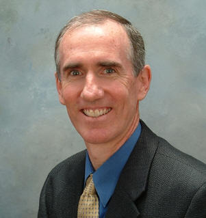
Christopher Henderson, President of Semitracks

Christopher Henderson

Christopher Henderson received his B.S. in Physics from the New Mexico Institute of Mining and Technology and his M.S.E.E. from the University of New Mexico. Chris is the President and one of the founders of Semitracks Inc., a United States-based company that provides education and semiconductor training to the electronics industry.

From 1988 to 2004, Chris worked at Sandia National Laboratories, where he was a Principal Member of Technical Staff in the Failure Analysis Department and Microsystems Partnerships Department. His job responsibilities have included failure and yield analysis of components fabricated at Sandia's Microelectronics Development Laboratory, research into the electrical behavior of defects, and consulting on microelectronics issues for the DoD. He has published over 20 papers at various conferences in semiconductor processing, reliability, failure analysis, and test. He has received two R&D 100 awards and two best paper awards. Prior to working at Sandia, Chris worked for Honeywell, BF Goodrich Aerospace, and Intel. Chris is a member of IEEE and EDFAS (the Electron Device Failure Analysis Society).

At Semitracks, Chris teaches courses on failure and yield analysis, semiconductor reliability, and other aspects of semiconductor technology.